GaN: Excelling in the extreme

Eradicating a high defect density in GaN epilayers will allow devices to shine in extreme environments, where they are adept at withstanding high temperatures, corrosive materials and bombardment from radiation.
BY SAVANNAH EISNER, JESSICA FRICK AND DEBBIE SENESKY FROM STANFORD UNIVERSITY
Thanks to its remarkable properties, GaN is now a mainstay material for power and RF electronics. Its cherished strengths are its high breakdown voltage, and its high values for the mobility and the carrier saturation velocity of its two-dimensional electron gas (2DEG) channel. But what makes this material even more remarkable is that it combines these attributes with a tolerance to high temperatures and a tremendous resistance to radiation attack – it is these attributes that make GaN a very attractive material for expanding the Internet of Things (IoT) into extreme environments.
This particular promise has not gone unnoticed, with researchers already starting to explore GaN as a platform for long-range IoT communication technology in space exploration applications, as well as medium-range IoT communication technologies in terrestrial applications requiring computation, timing, and sensing within hostile conditions. There are emerging opportunities for GaN associated with geothermal, oil and gas, and hypersonics.
GaN can be harnessed for all of these opportunities because silicon, the dominant semiconductor of choice for many decades, exhibits poor performance in extreme environments. Since its invention in 1954, the scope of the silicon transistor has been fundamentally limited to benign environments.
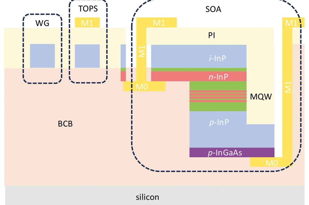
Cross-sectional schematic of the (a) InAlN/GaN HEMTs, (b) InAlN/GaN
Hall-effect sensors, and (c) AlGaN/GaN UV photodetectors exposed to the
Venus-simulant environment. Interfaces where the 2DEG is present are
represented by white dashed lines. Reproduced from S. R. Eisner et al.,
“Extended Exposure of Gallium Nitride Heterostructure Devices to a
Simulated Venus Environment,” 2021 IEEE Aerospace Conference (50100),
Big Sky, MT, USA, 2021, pp. 1-12.
Due to a bandgap of around just 1.2 eV, devices made from silicon are incapable of operating at temperatures above around 200 °C. This severe limitation causes silicon devices and circuits to require active cooling to operate in harsh environments.
Note, though, that moving beyond silicon offers far more than just simplifying thermal management. As electronic applications become more power dense, platforms based on a successor to silicon can cater to this need, while also functioning reliably and not requiring complex, expensive packaging. Enabling these capabilities has tremendous value, given the strict payload and cost requirements of modern-day engineering systems.
Superior alternatives to silicon are not limited to GaN, but encompass a number of other wide bandgap materials, such as SiC and diamond. All offer higher power densities, as well as lower power consumption.
In the case of GaN, the material attributes that enable power-efficient, high-frequency operation are also behind the compelling initial demonstrations of device operation in hot ambients. The heterostructured InAlN/GaN platform has already reached an eye-watering operating temperature of 1000 °C, a remarkable feat that’s enabled by complementary high-temperature metal contacts and reduced strain relaxation effects.
Such a performance is impossible to realise in silicon, because its intrinsic carrier concentration is too high to ensure current modulation at high temperatures. Under this condition, the carriers in silicon that are thermally activated into the conduction band would overwhelm the channel. GaN does not suffer the same fate, thanks to a bandgap that is three times wider, and a lower intrinsic carrier concentration.
A much desired, unique feature of the GaN material system is the polarisation-induced formation of the 2DEG channel at the heterointerface. Thanks to these polarisation effects, it is possible to form a conducting channel without doping. The major implication is that the channel in GaN devices is free from deleterious dopant scattering and diffusion, known to negatively impact device performance at high and low temperatures. The two-dimensional channel in GaN heterostructures can support very high electron mobilities, on the order of 2200 cm2 V-1 s-1, at room temperature.
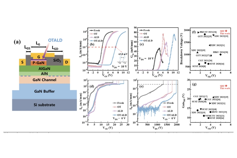
InAlN/GaN HEMT transfer characteristics before and after 10-day exposure
in a Venus simulation chamber. Reproduced from S. R. Eisner et al.
“Extended Exposure of Gallium Nitride Heterostructure Devices to a
Simulated Venus Environment,” 2021 IEEE Aerospace Conference (50100),
Big Sky, MT, USA, 2021, pp. 1-12.
The merits of GaN heterostructures with a 2DEG have inspired a multitude of demonstrations of solid-state and MEMS sensors at the micro- and nano-scale. Opportunities for GaN resonators that utilise a 2DEG for piezoelectric transduction include (1) deployment in harsh-environments, for infrared and chemical sensing, and (2) in oscillators, to provide stable, chip-scale clocks for a GaN-based IoT platform. Other exciting developments include: micro-pressure sensors fabricated in GaN heterostructured membranes, shown to work at up to 300 °C in air; mechanical sensors for harsh environments, such as seismometers, accelerometers, gyroscopes; and strain sensors, which can similarly benefit from strain transduction in GaN. There’s also opportunity for high-gain UV photodetectors, exploiting the valence band offset in GaN heterostructure epitaxial layers, with devices formed using 2DEG interdigitated electrodes. And this list goes on - magnetic field sensing capabilities with high sensitivities have been achieved in both AlGaN/GaN and InAlN/GaN; and heterostructured GaN has demonstrated energy harvesting capabilities in extreme environments, through thermoelectrics and betavoltaics. It’s also possible to amplify signals from these sensors without having to introduce another material system, because signal amplification and logic can be performed by the well-known GaN HEMT.
Thanks to the lateral layout of the GaN heterostructure, as well as compatible microfabrication processes, the plethora of sensors that can be produced are amenable to monolithic integration. Due to this, it is possible to produce single, uncooled heterostructured GaN chips that combine sensing, communication, and power functionality; can operate for long durations in extreme environments while connecting with an IoT network; and have no need for cooling or shielding. In addition to these assets, such monolithically-integrated electronics yield lighter, cheaper IoT systems.
Custom Venus simulation chamber for subjecting devices to realistic
harsh environmental conditions in the Extreme Environment Microsystems
Lab (XLab) at Stanford University.
Venturing to Venus
One exciting new frontier in space exploration that can be unlocked by leveraging GaN IoT technology is a long-lived mission to the hostile surface of Venus. This heavenly body is often called Earth’s ‘sister planet’, due to its similar size, composition, and relative position in the solar system.
The majority of Venus surface exploration programmes date back to the 1970s and 1980s, led by the Soviet Union. Of those, the longest-lived Venus surface mission, Venera 13, lasted just over 2 hours. To put that timespan into perspective, the record lifetime of a Mars surface mission stands at 14 years and 138 days, set by NASA’s Opportunity rover between 2004 and 2018.
The staggering discrepancy in the mission lengths on the surfaces of Venus and Mars is a poignant reflection of the massive technical hurdle to exploration presented by the inhospitable Venus environment. While there may be planetary similarities between Venus and Earth, the climates are utterly different. The surface of Venus is a blistering 464 °C, and atmospheric pressure is over 90 bars – that’s equivalent to the pressure found at a depth of 1 km in our oceans. The content of the atmospheres is also dissimilar, with that for Venus consisting mainly of corrosive CO2, rendered into a supercritical state by high temperature and pressure. Other constituents of Venus’ atmosphere include nasty, corrosive and caustic chemical compounds, such as SO2 and hydrofluoric and hydrochloric acids.
This toxic composition, allied to extreme physical conditions, creates a hostile surface that exceeds the operational limits of traditional silicon microelectronics, making robotic exploration missions exceptionally technologically challenging. Silicon falls well short of what’s needed on many fronts, as it’s chemically incompatible with Venus’ atmosphere, and incapable of operating at this planet’s surface temperatures, even with the introduction of strategic technologies, such as silicon-on-insulator. Applying active cooling and shielding measures makes little difference, as evidenced by the transmission failure of the silicon microelectronics on board Venera 13 after reaching ambient temperature.
In the decades since the last dedicated Venus surface mission – the Soviet’s 1985 Vega 1 mission – scientific study of this planet has focused on orbiting spacecraft and satellites, primarily on fly-by missions to other destinations. While such an approach garners useful information, insight is hampered by a very thick cloud layer that surrounds the planet and prevents scientists from answering many of the outstanding questions about Venus.
GaN heterostructure devices being tested at 600 °C in air in the Extreme
Environment Microsystems Lab (XLab) at Stanford University.
Revived by NASA
Priorities for what should be discovered on a future mission have been identified by NASA’s Venus Exploration Analysis Group (VEXAG). This group has highlighted the need for studies of mineralogy, seismology, metrology, and chemical interactions between the surface and the atmosphere. To obtain sufficient information, the length of the mission needs to far exceed that of Venera 13 – the time scale should be weeks or months – to enable observations that cover various times of the day and differing weather conditions. An extended duration mission would deliver an additional benefit, as it would allow for remote, human-in-the-loop decision-making capabilities. This is the case with Mars surface rovers, with a team on Earth determining where to drill and conduct sample analysis.
The scientific knowledge gained from such a mission is not limited to expanding our knowledge of Venus. This endeavour would also shed new light on the factors that influence diversity in planetary bodies, including greater insight into the drivers behind the divergence in the evolution of Earth and Venus, and why these two support different climates and geological features. Despite its extreme environment today, there may have been a time when Venus hosted ancient oceans, and perhaps even life on its surface. The extent and timespan of these oceans is still debated. By increasing our understanding of Venus, which suffers from a runaway greenhouse gas effect, we may resolve this debate while gaining a better understanding of similar processes, and the impact they might have here on Earth. Achieving these objectives could help shape our criteria when searching for other potentially habitable exo-planets.
Savannah Eisner beside the Stanford Nanofabrication Facility’s Aixtron
MOCVD III-N System growing epitaxial GaN heterostructure thin films.
For a Venus surface mission, the desired instrumentation requires multiple semiconductor devices. They are needed for: sensors and imagers; mass and laser spectrometer control and read-out electronics; low-power sample handling processors needed to command a drill; and for power system electronics, to control switching and power distribution. Thanks to the potential for monolithic integration in GaN heterostructures, a future mission to Venus may include large-scale surface exploration, carried out by multiple robotic rovers, which generate large amounts of sensor data and communicate, via the IoT, with each other and orbiting satellites.
The prospects of such missions are on the rise, with Venus surface exploration recently garnering increasing support. NASA has just awarded funding to two new missions to explore Venus through the Discovery programme. While neither DAVINCI+ (Deep Atmosphere Venus Investigation of Noble gases, Chemistry, and Imaging) nor VERITAS (Venus Emissivity, Radio Science, InSAR, Topography, and Spectroscopy) will lead to instrumentation on the surface of this planet, these programmes represent the beginning of what may be an exciting new chapter in Venus exploration. One hope is that they will ultimately lend credence to future surface study mission concepts demanding IoT capabilities. Efforts in this direction would have additional benefits, as they would support missions to other hot planetary bodies like Mercury or gas giants – such ventures would value uncooled instrumentation technologies enabled by heterostructured GaN.
GaN’s Achilles heel
Unfortunately, the innate robustness of GaN that makes it ideal for operating in extreme environments – its tolerance to high temperatures and resistance to radiation damage and chemical attack – comes at a price. The downside is that GaN is challenging to synthesize. The promising results realised with GaN micro/nanoelectronics in terms of high power, high frequency, and high temperature tend to rely on epitaxial growth of thin films on foreign substrates, such as those made from silicon, sapphire, or SiC. Growth on these non-native foundations leads to relatively high defect densities in the epilayers that present challenges to extreme environment operation.
Shortfalls in performance, stemming from the relatively high defect densities, include compromised reliability, seen in the likes of high off-state leakage currents and trapping related phenomenon, such as current collapse. Another downside of the high defect density and resulting traps is a transient persistent photoconductivity, which degrades the light sensing capabilities in GaN. As well as plaguing lateral heterostructured GaN 2DEG devices, defect-related issues present a challenge to vertical device architectures, which are desirable for high-power applications.
The obvious solution is to slash the defect density in devices. Switching the foundation for growth to GaN should address this, but it is challenging to realise cost-effective growth of native bulk GaN substrates and epitaxial layers.
Current-scaled sensitivity of (a) InAlN/GaN and (b) AlGaN/GaN
Hall-effect magnetic field sensors between room temperature and 576 °C
in air. Reproduced from H.S. Alpert et al. Rev Sci Instrum. 91 025003
(2020)
A lack of progress on this front is not a reflection of a lack of effort. For many years, a number of research groups around the world have been pursuing the growth of single-crystal GaN substrates. But as some would say, GaN substrates remain ‘hard to break, hard to make’. This state-of affairs stems from the relationship between the composite elements, Ga and N, which differ in electronegativity by 1.2 – that high value reflects the highly polar covalent nature of the bonds. Such bonding accounts for melting at the extreme conditions of around 2500 °C and 4.5 GPa. Drop below this pressure and rather than melting, GaN decomposes into liquid gallium and nitrogen gas.
To circumvent the need for extremely high processing pressures, which are incompatible with today’s industrial capabilities, GaN is produced by three standard methods: halide vapor phase epitaxy (HVPE), ammonothermal, and sodium-flux. Of these three, ammonothermal is the most consistent in producing relatively large-scale bulk GaN wafers. In 2021, a partnership between the Japanese Steel Corporation and Mitsubishi Chemical Corporation reported the production of 4-inch bulk GaN wafers, the largest size grown to date using the ammonothermal method. Ammonothermal reactions are a specific subset of solvothermal synthesis – where an organic liquid phase interaction is heated in a pressure-safe vessel above its boiling point. In the case of ammonothermal reactions, ammonia provides the solvent in the presence of liquid gallium.
2DEG sheet density of InAlN/GaN and AlGaN/GaN samples from room
temperature to 576 °C. The inset shows the AlGaN/GaN 2DEG sheet density
over temperature on tighter axes. Reproduced from H.S. Alpert et al. Rev
Sci Instrum. 91 025003 (2020)
Like all liquid-phase reactions, ammonothermal synthesis is prone to gravity-induced phenomena. They include: container interactions, thermal convection, buoyancy, and sedimentation. All actively work against the formation of low-defect, large diameter, single crystals. The hope is that new in-space manufacturing capabilities will remove gravity from the synthesis and unlock high-quality, commercial-scale GaN wafers. Semiconductor synthesis in space is an exciting new frontier tipped to play a crucial role for many decades in the ‘beyond silicon’ era.
Main picture credit NASA


