
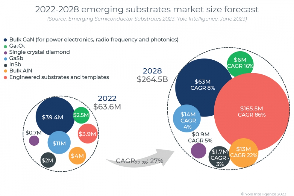
Substrates market to exceed $264M by 2028
But which emerging semiconductor substrate will be the next game changer?
In the previous decade, compound semiconductors such as GaAs for RF and SiC for power electronics entered the mass market. Which emerging semiconductor substrate will be the next game changer?
In a new report, Yole investigates the status of emerging semiconductor substrates, including GaSb, InSb, bulk GaN, Ga2O3, bulk AlN, and diamond, as well as engineered substrates and templates. Furthermore, it looks at various potential applications such as power electronics, RF, and photonics are covered, including laser diodes, LEDs, sensors, and detectors.
The power electronics (PE) market, driven by several applications such as electric and hybrid electric vehicles (EV/HEV), renewable energy, and power supplies, is still dominated by Silicon-based technologies. Nevertheless, the wide bandgap materials SiC and GaN (Lateral GaN HEMT on Si or Sapphire) have penetrated the PE market after a long development process and are expected to constitute more than 25 percent of the market by 2028. Benefitting from this momentum, Yole expecst bulk GaN for vertical GaN devices and engineered substrates (SmartSiC from Soitec, SiCkrest from SICOXS, and QST from Qromis) to grow in the coming five years.
Photonics, on the other hand, enjoys stable growth with GaSb-based devices such as IR lasers and imagers driven mainly by high-end and niche military applications. While GaSb is growing, what is the market status of InSb? Concerning the bulk GaN substrates in consumer, industrial, and automotive applications, the market is considered stable with a stronger push into industrial applications. During the pandemic outbreak, UVC disinfection/purification systems started using bulk AlN substrates. According to Yole, this could drive the AlN substrates market to a CAGR2022-2028 of 22 percent, the highest among all the emerging photonics substrates.
Supply chain questions
Generally speaking, the supply chain for emerging substrates is not well established. It is dominated by start-ups and spin-offs from research groups that have developed know-how during academic R&D activities and are willing to transfer it to industry. Considerable investments and risk-taking from established big players are needed for an emerging substrate market to ramp up.
In the power electronics ecosystem, Ga2O3, bulk GaN, diamond, and engineered substrates are proposed for developing highly efficient devices and systems. Engineered substrates and bulk GaN are expected to grow significantly in the next five years, profiting from the growth of wide bandgap materials.
Established players like STMicroelectronics are already working with SOITEC for the supply of their SmartSiC engineered substrates. Qromis is partnering with Vanguard International Semiconductor and ShinEtsu to manufacture and offer GaN-on-QST engineered substrates.
The Ga2O3 substrate supply chain is more dominated by start-ups, with established players showing less interest. Regarding the use of diamond, the entry of established players from the jewelry business, like Diamond Foundry, may positively impact the availability of large wafer sizes and increase production capacity.
In the photonics ecosystem, the GaSb and InSb substrate markets are well-established and dominated by two leading players, IQE and IntelliEPI. The situation is quite similar for bulk GaN substrates, with the Japanese players Sumitomo Chemical and Mitsubishi Electric dominating the market. On the other hand, the bulk AlN substrates business is not well established. Yole sese two Japanese device players, Stanley Electric and Asahi Kasei, acquiring two US substrate players, Hexatech and Crystal IS, respectively. Both parent companies are aiming to increase their market share, decrease costs, and secure the supply of expensive bulk AlN substrates.
Larger diameter, better quality

Emerging substrate activities focus mainly on technological development for better material quality, higher yields, and lower production costs. This push needs, of course, to be supported by market demand and adoption in volume applications which defines the correct specification of the different substrates.
For power electronics, at least a 6-inch wafer size is needed for established foundries to be involved at high volumes. This pushes the substrate players to optimise the manufacturing techniques to increase the wafer sizes. For diamond, the mosaic diamond method from EDP, which delivers up to 28 x 28 mm², and heterogeneous diamond growth on Si or sapphire substrates from Orbray or Audiatec up to around 6-inch diameter, have been developed. In addition, 6-inch Bulk GaN substrates have been demonstrated using HVPE and other techniques, though more work is still needed to improve the material quality and meet application requirements.
Similarly, for Ga2O3, different melt growth techniques are being used, with EFG the most promising to obtain 6-inch wafers with acceptable material quality at volume production. Regarding engineered substrates, advanced splitting and bonding techniques are used to overcome challenges for larger single-crystal substrates and better material quality.
For photonics, the GaSb and InSb mainstream substrate sizes are 3- and 4-inch despite the commercial availability of 5- and 6-inch. This is due to the niche applications for antimonides. However, the story is different for bulk GaN and AlN: the transition to a larger substrate diameter, from 2-inch to 3- and 4-inch, is driven by the goal of reducing the cost per device.
Bulk GaN substrate players such as Sumitomo Chemical and Mitsubishi Chemical have demonstrated 4-inch and 6-inch substrates for photonics applications; however, market adoption is slow due to the quality issues of these substrates and the low-volume applications. On the other hand, AlN substrate players such as Crystal IS and Ultratrend technologies have already demonstrated 3-inch AlN substrates, while Hexatech announced investments in 2022 to accelerate the adoption of 4-inch AlN substrates in the market.


