
CEA-Leti and Intel to develop 2D TMDs on 300mm wafers
Joint research project aims to extend Moore’s Law beyond 2030
CEA-Leti and Intel have announced a joint research project to develop layer transfer technology of two-dimensional transition-metal dichalcogenides (2D TMDs) on 300mm wafers with the goal to extend Moore’s Law beyond 2030.
2D-layered semiconductors, such as molybdenum- and tungsten-based TMDs, are promising candidates to extend Moore’s Law and ensure ultimate scaling of MOSFET transistors, because 2D-FETs provide innate sub-1nm transistor channel thickness. They are suitable for high-performance and low-power platforms due to their good carrier transport and mobility, even for atomically thin layers. In addition, their device body thickness and moderate energy bandgap lead to enhanced electrostatic control, and thus, to low off-state currents.
These characteristics position 2D-FET stacked-nanosheet devices as a promising solution for transistor scaling beyond 2030, which will require high-quality 2D channel growth, adapted transfer and robust process modules. To that end, the multi-year project will develop a viable layer-transfer technology of high-quality 2D materials (grown on 300mm preferred substrates) to another device substrate for transistor process integration. Intel brings decades of R&D and manufacturing expertise to this project and CEA-Leti also provides bonding and transfer-layer expertise and large-scale characterisation.
“As we are relentlessly pushing Moore’s Law, 2D TMD material is a promising option for extending the limits of transistor scaling in the future,” said Robert Chau, Intel senior fellow in Technology Development and firector of Intel Europe Research. “This research program focuses on developing a viable 2D TMD-based technology in 300mm for future Moore’s Law transistor scaling.”
Intel brings its prowess and expertise in semiconductor-and-packaging research and technology to work with European partners to develop Moore's Law innovations and advance microelectronics in Europe. In 2022, Chau relocated from the U.S. to Europe to lead Intel Europe Research and to drive the Intel’s R&D with partners on the continent. Intel and CEA-Leti have a long history of strong collaboration in semiconductor design, processes and packaging technology.
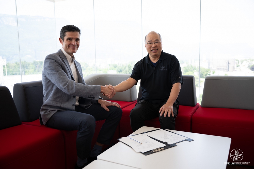
Most recently, they announced a research breakthrough in a new die-to-wafer bonding technology using a self-assembly process for future chip integration in June 2022. Chau, who visited CEA-Leti’s Grenoble headquarters on June 16 for the launch of the project, has been a strong supporter of multi-year research collaborations between the two entities.
CEA-Leti CEO Sebastien Dauvé said industry roadmaps show that 2D materials will be integrated in future microelectronic devices, and transfer capability in 300mm wafers will be key to that integration.
“Due to their high-growth temperature exceeding 700°C and high-quality growth on preferred substrates, it is difficult to stack 2D materials can hardly be deposited on a stack as usual thin layers. So transfer holds the most promise for integrating them in future devices, and CEA-Leti’s strengths in this context are its expertise and know-how in transfer development and characterisation,” Dauvé said.


