Loading...
News Article

DISCO develops KABRA process for GaN wafers

News

Process can increase the number of GaN wafers produced and decrease production time

DISCO Corporation has developed a KABRA ingot slicing method specially optimised for the production of GaN wafers.

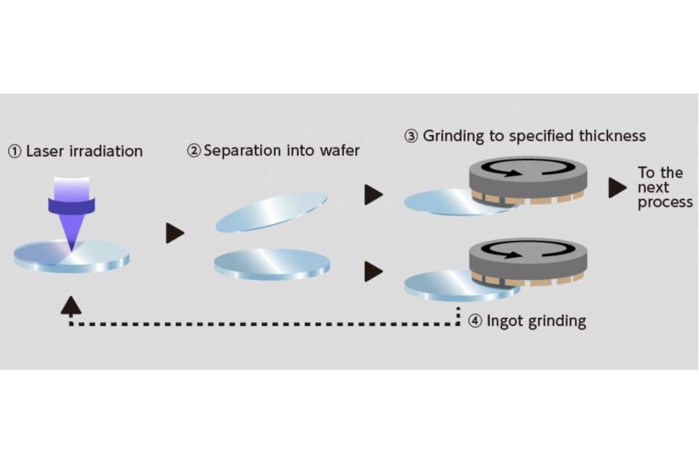
In the KABRA process (shown above), a separation layer (KABRA layer) is formed at a specified depth by continuously irradiating an ingot with a laser, producing wafers starting from the KABRA layer.

This approach can increase the number of GaN wafers produced and decrease production time, according to DISCO.

GaN requires time for crystal growth, and is a very delicate material as the ingots produced are small in diameter and thin. Conventionally, the mainstream method to slice GaN ingots into wafers is to use a diamond wire saw. However, the are problems when slicing with a wire saw, such as the processing time, material loss at the sliced sections that is thicker than the thickness of the wire used, and a low number of wafers produced due to material loss from the lapping process which is done after slicing to planarise the surface.

From the time when the KABRA process was developed for the production of SiC wafers, DISCO says it has been receiving requests from many manufacturers to apply this process to GaN as well.

DISCO has since been putting effort into R&D in order to realise a KABRA process optimised for GaN, and has now introduced it for mass-production.
QD company Quantum Science expands into new facility
Innoscience files lawsuit against Infineon
Riber revenues up 5% to €41.2m
Forvia Hella to use CoolSiC for next generation charging
Photon Design to exhibit QD simulation tool
Ortel transfers CW laser fabrication to Canada
Luminus adds red and blue multi-mode Lasers
PseudolithIC raises $6M for heterogeneous chiplet tech
Mesa sidewall design improves HV DUV LEDs
IQE revenue to exceed expectations
'Game-changing' VCSEL system targets clinical imaging
German start-up secures finance for SiC processing tech
Macom signs preliminaries for CHIPS Act funding
IQE and Quintessent partner on QD lasers for AI
EU funds perovskite tandems for fuel-free space propulsion
EU to invest €3m in GeSi quantum project
Transforming the current density of AlN Schottky barrier diodes
Turbocharging the GaN MOSFET with a HfO₂ gate
Wolfspeed launches Gen 4 SiC MOSFET technology
Report predicts high growth for UK's North East
Element Six unveils Cu-diamond composite
SemiQ launches hi-rel 1700V SiC MOSFETs
Lynred to exhibit Eyesential SWIR sensor for machine vision
Thorlabs buys VCSEL firm Praevium Research
Advancing tuneable InP lasers on a heterogeneous platform
P-GaN gate HEMTs have record threshold voltage
Guerrilla RF releases GaN power amplifier dice
Narrow-linewidth DFB lasers now at 405 and 488nm
Researchers develop tech for future fast-charging stations
Vermont GaN Tech Hub awarded nearly $24M
Onsemi completes buy-out of Qorvo SiC JFET business
Quantum Science announces Innovate UK funding
×
Search the news archive

To close this popup you can press escape or click the close icon.
Logo
x
Logo
×
Register - Step 1

You may choose to subscribe to the Compound Semiconductor Magazine, the Compound Semiconductor Newsletter, or both. You may also request additional information if required, before submitting your application.


Please subscribe me to:


You chose the industry type of "Other"

Please enter the industry that you work in:
 
x
Adblocker Detected
Please consider unblocking adverts on this website