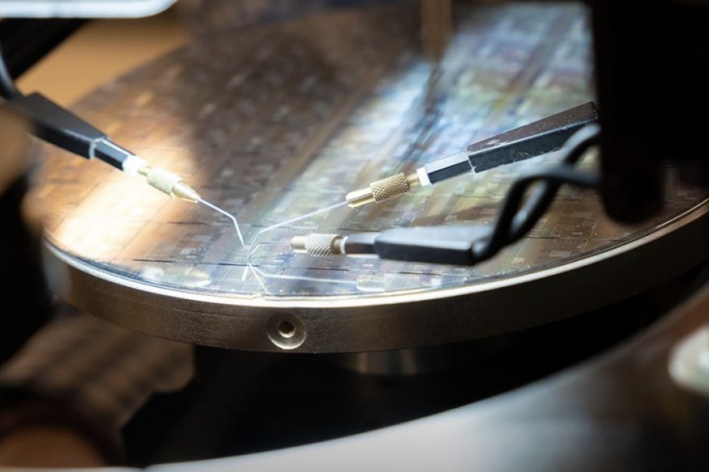
Indian GaN centre installs Oxford Instruments tools

GaN Ecosystem Enabling Centre and Incubator orders full suite of plasma processing solutions for power & RF pilot line
Oxford Instruments Plasma Technology has announced a substantial equipment shipment to the GaN Ecosystem Enabling Centre and Incubator (GEECI) located at the Centre for Nano Science and Engineering, (CeNSE) Indian Institute of Science (IISc), in Bengaluru (formally Bangalore).
The technologies being installed in the pilot production line include atomic layer etch (ALE), two variants of inductively coupled plasma (ICP) etch modules, and plasma enhanced chemical vapour deposition (PECVD). The suite of GaN plasma processing solutions will be used to develop next generation GaN-on-Si and GaN-on-SiC high power and high frequency power electronics and RF devices to offer improved efficiency and performance.
The market size for GaN is projected to be >$2B annually by 2027. GaN offers many device performance benefits in the RF and power electronics space, like advantages in power density, bandwidth, efficiency and thermal conductivity, but more research into stress and defects of the material and their impact at device level, is required to further accelerate its adoption across all markets.
Positioned within India’s premier high technology hub, in the city of Bengaluru and with strong links to several technology giants within the hub, GEECI is an ideal environment for technology start-ups and spin-offs.
Srinivasan Raghavan (Vasu), who is charge of setting up GEECI, said: “The equipment, ongoing process and service support, and technical collaboration with Oxford Instruments Plasma Technology is crucial to our GaN device development program. We are incredibly excited to partner with Oxford Instruments to establish our new GaN pilot production line to support the next generation of GaN startups and spin outs, which are critical to accelerate India’s flourishing semiconductor ecosystem.
Shankar Kumar Selvaraja the Process expert said, “We look forward to developing new process recipes to enable GaN power and RF electronics”.
Ian Wright, Plasma Technology’s VP of sales and business development, Asia, commented: “We are delighted to be bringing our GaN technology to such a prestigious institution as the IISc. We have recently experienced a surge in interest for our solutions in India, which points toward a shift in the technology landscape for that region with momentum generated through government funding,” also commenting, “We have invested in an ambitious and expanding program of service and support for India, and are uniquely positioned in the region, to play an integral role in encouraging transformational semiconductor technology development and industry growth.”


