Loading...
News Article

Micro-transfer printing for heterogeneous PICs

News

Belgian group develops versatile, widely applicable micro-transfer printing technology

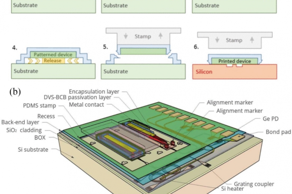
A group of researchers from the University of Ghent in Belgium has developed a new integration approach for heterogeneous silicon photonic integrated circuits (PICs). They say their micro-transfer printing (μTP) approach combines the high throughput advantages of die-to-wafer bonding with those of flip-chip integration.

The researchers describe the process rather like pressing a stamp down on paper. The stamp is 65 percent polydimethylsiloxane (PDMS), a transparent material, which is used to transfer the components into a substrate with 1 μm lateral alignment tolerance.

Transfer printing is used because is easier and cheaper to make III-V devices on a native substrate. The Belgian researchers also use III-V materials for their waveguides. Ultimately though, all these parts must go onto a silicon substrate.

The transfer technology is said to be very versatile. Other demonstrations of μTP are underway, specifically: InAs/GaAs quantum dot lasers, Ce:YIG magneto-optic materials for optical isolators, periodically poled LiNbO3 for nonlinear optics, BiCMOS electronics. Scaling up the technology to 200 mm and 300 mm wafers is underway.

The researchers say they are continuously improving device performance (e.g., laserwall plug efficiency) and studying yield and reliability. However, there is still a way to go for this technology to be used as a manufacturing technology.

Reference

'Micro-Transfer Printing for Heterogeneous Si Photonic Integrated Circuits' by G. Roelkens et al; IEEE Journal of Selected Topics in Quantum Electronics, vol. 29, no. 3: Photon. Elec. Co-Inte. and Adv. Trans. Print., pp. 1-14, May-June 2023

QD company Quantum Science expands into new facility
Innoscience files lawsuit against Infineon
Riber revenues up 5% to €41.2m
Forvia Hella to use CoolSiC for next generation charging
Photon Design to exhibit QD simulation tool
Ortel transfers CW laser fabrication to Canada
Luminus adds red and blue multi-mode Lasers
PseudolithIC raises $6M for heterogeneous chiplet tech
Mesa sidewall design improves HV DUV LEDs
IQE revenue to exceed expectations
'Game-changing' VCSEL system targets clinical imaging
German start-up secures finance for SiC processing tech
Macom signs preliminaries for CHIPS Act funding
IQE and Quintessent partner on QD lasers for AI
EU funds perovskite tandems for fuel-free space propulsion
EU to invest €3m in GeSi quantum project
Transforming the current density of AlN Schottky barrier diodes
Turbocharging the GaN MOSFET with a HfO₂ gate
Wolfspeed launches Gen 4 SiC MOSFET technology
Report predicts high growth for UK's North East
Element Six unveils Cu-diamond composite
SemiQ launches hi-rel 1700V SiC MOSFETs
Lynred to exhibit Eyesential SWIR sensor for machine vision
Thorlabs buys VCSEL firm Praevium Research
Advancing tuneable InP lasers on a heterogeneous platform
P-GaN gate HEMTs have record threshold voltage
Guerrilla RF releases GaN power amplifier dice
Narrow-linewidth DFB lasers now at 405 and 488nm
Researchers develop tech for future fast-charging stations
Vermont GaN Tech Hub awarded nearly $24M
Onsemi completes buy-out of Qorvo SiC JFET business
Quantum Science announces Innovate UK funding
×
Search the news archive

To close this popup you can press escape or click the close icon.
Logo
x
Logo
×
Register - Step 1

You may choose to subscribe to the Compound Semiconductor Magazine, the Compound Semiconductor Newsletter, or both. You may also request additional information if required, before submitting your application.


Please subscribe me to:


You chose the industry type of "Other"

Please enter the industry that you work in: