Loading...
News Article

Applied Materials and Fraunhofer IPMS launch metrology hub

News

New hub aims to accelerate semiconductor research and enhance development projects

Applied Materials, and the Fraunhofer Institute for Photonic Microsystems IPMS, have announced a collaboration to create Europe´s largest technology hub for semiconductor metrology and process analysis.

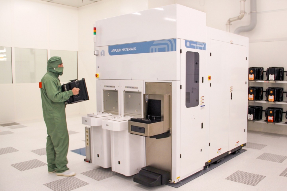
To be located at the Center Nanoelectronic Technologies (CNT) of Fraunhofer IPMS in Dresden, the technology hub is situated in the heart of Silicon Saxony, Europe’s largest semiconductor cluster. The hub will be equipped with Applied Materials’ eBeam metrology equipment, including its VeritySEM CD-SEM (critical dimension scanning electron microscope) systems, and staffed by Applied engineers and R&D experts.

“Fraunhofer IPMS and its partners will benefit from access to Applied’s industry-leading eBeam metrology systems”, said Benjamin Uhlig-Lilienthal, Head of Business Unit Next Generation Computing at Fraunhofer IPMS. “The new technology hub will offer advanced wafer-level metrology in our industrial CMOS environment with Fraunhofer IPMS’s unique ability to loop wafers directly with semiconductor manufacturers.”

“Our collaborative metrology hub will accelerate learning cycles and the development of new applications for the Fraunhofer Institute, Applied Materials and our customers and partners in Europe,” said James Robson, corporate VP for Applied Materials Europe. “This unique technology hub will have the capability to test and qualify processes on a variety of substrate materials and wafer thicknesses critical to applications across the diverse European semiconductor landscape.”

QD company Quantum Science expands into new facility
Innoscience files lawsuit against Infineon
Riber revenues up 5% to €41.2m
Forvia Hella to use CoolSiC for next generation charging
Photon Design to exhibit QD simulation tool
Ortel transfers CW laser fabrication to Canada
Luminus adds red and blue multi-mode Lasers
PseudolithIC raises $6M for heterogeneous chiplet tech
Mesa sidewall design improves HV DUV LEDs
IQE revenue to exceed expectations
'Game-changing' VCSEL system targets clinical imaging
German start-up secures finance for SiC processing tech
Macom signs preliminaries for CHIPS Act funding
IQE and Quintessent partner on QD lasers for AI
EU funds perovskite tandems for fuel-free space propulsion
EU to invest €3m in GeSi quantum project
Transforming the current density of AlN Schottky barrier diodes
Turbocharging the GaN MOSFET with a HfO₂ gate
Wolfspeed launches Gen 4 SiC MOSFET technology
Report predicts high growth for UK's North East
Element Six unveils Cu-diamond composite
SemiQ launches hi-rel 1700V SiC MOSFETs
Lynred to exhibit Eyesential SWIR sensor for machine vision
Thorlabs buys VCSEL firm Praevium Research
Advancing tuneable InP lasers on a heterogeneous platform
P-GaN gate HEMTs have record threshold voltage
Guerrilla RF releases GaN power amplifier dice
Narrow-linewidth DFB lasers now at 405 and 488nm
Researchers develop tech for future fast-charging stations
Vermont GaN Tech Hub awarded nearly $24M
Onsemi completes buy-out of Qorvo SiC JFET business
Quantum Science announces Innovate UK funding
×
Search the news archive

To close this popup you can press escape or click the close icon.
Logo
x
Logo
×
Register - Step 1

You may choose to subscribe to the Compound Semiconductor Magazine, the Compound Semiconductor Newsletter, or both. You may also request additional information if required, before submitting your application.


Please subscribe me to:


You chose the industry type of "Other"

Please enter the industry that you work in: