
Refining GaN substrate thinning
Switching to a hydrogen-based plasma ensures high-speed etching of GaN substrates
Engineers at Osaka University, Japan, are claiming to have broken new ground by thinning GaN substrates with a hydrogen-based plasma.
The team’s technique, which is capable of an etching rate of up to 4 µm/minute, provides a promising approach to thinning the substrate of vertical power devices. This is needed to trim the on-resistance of vertical devices, and enable them to compete for deployment in electric vehicles.
The approach that is being pioneered by the team at Osaka University is a compelling alternative to established mechanical machining processes, such as grinding and polishing – both are used today to thin substrates. These mechanical methodologies work well when providing thinning for silicon power devices, but struggle when employed for the likes of SiC and GaN, due to issues such as cracking, chipping and warping.
To thin GaN substrates, the engineers at Osaka University use an approach known as plasma chemical vaporisation machining (PCVM), which they have been employing and refining for more than 25 years.
“Initially we were processing silicon wafers, SOI wafers and silicon X-ray mirrors for synchrotron radiation,” remarks team spokesperson Yasuhisa Sano. They started processing SiC substrates about 15 years ago, and in recent years they began to process GaN and Ga2O3 substrates.
One distinguising feature of PCVM is the use of a plasma pressure of several tenths of an atmosphere, which ensures a short mean path for the gas molecules and a low energy for the ions. Due to this, reactive species are not ions, but neutral radicals, which do not disrupt the atomic arrangement of the processed surface and do not warp the substrate.
Back in 2021, Sano and co-workers reported the thinning of a 2-inch SiC substrate by PCVM at a rate of 15 µm/minute, using SF6 gas. Unfortunately, it’s not possible to apply this approach directly to GaN, because SF6 gas does not ensure etching. And chlorine-based gases, obvious contenders, are also unsuitable, because they have a corrosive nature that threatens to damage the surface of GaN devices.
These issues led the team to consider using hydrogen. Offering encouragement that this might lead to success is the use of hydrogen gas in HVPE growth of GaN, and the exitance of the gas digalane (Ga2H6).
Investigations involving hydrogen began with a homemade 13.56 MHz RF plasma generator, incorporating a pipe-shaped electrode with a 2 mm outer diameter and a 0.3 mm hole diameter, and a 0.4 mm-thick, 2-inch GaN substrate.
Initially, the team looked into variations in removal rate after 5 minutes, using a helium-to-hydrogen ratio of 9:1, a flow rate of 100 sccm, and RF powers of 130 W, 150 W, 180 W and 200 W. This experiment, which also considered the substrate temperature, determined that a higher power is the main driver for increasing the removal rate – it increases the number of hydrogen radicals.
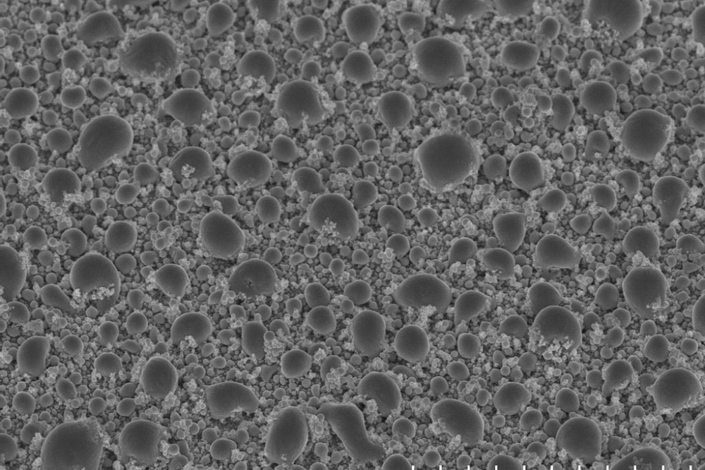
Sano and co-workers went on to consider the impact of the gas flow rate, with power fixed at 180 W. They compared the etching rates at flows of 100 sccm, 500 sccm and 800 sccm, this time at a helium-to-hydrogen ratio of 19:1, shown to speed the process according to preliminary investigations. At the highest flow, etching hit 4 µm/minute, but impacted surface quality, creating what is described as a pearskin surface (see figure above).
The team attribute this morphology to spherical deposits of gallium, which may be removed by heating the surface to 40 °C and wiping it. But there is a more elegant solution: adding oxygen gas to the process. Its introduction ensured a glossy surface with a roughness of just 0.9 nm, according to atomic force microscopy.
The team are now trying to establish the process conditions for obtaining good surface roughness, according to Sano. “At the same time, efforts are being made to process a larger area, in order to bring [our technique] closer to practical application.”
Reference
Y. Sano et al. Appl Phys. Express 16 045504 (2023)


