Loading...
News Article

Could silicon outperform GaAs in photodetectors?

News

US researchers show how silicon 'sponge' approach could dramatically increase photon absorption

Silicon is not a great material for photonic applications because it shows poor absorption of near-infrared light compared to compound semiconductors such as GaAs. On the other hand, GaAs is difficult to integrate with silicon microelectronics.

Now Saif Islam and colleagues at the UC Davis Department of Electrical and Computer Engineering have come up with an approach that dramatically increases the photon absorption of silicon. The work was published July 24 in Advanced Photonics Nexus.

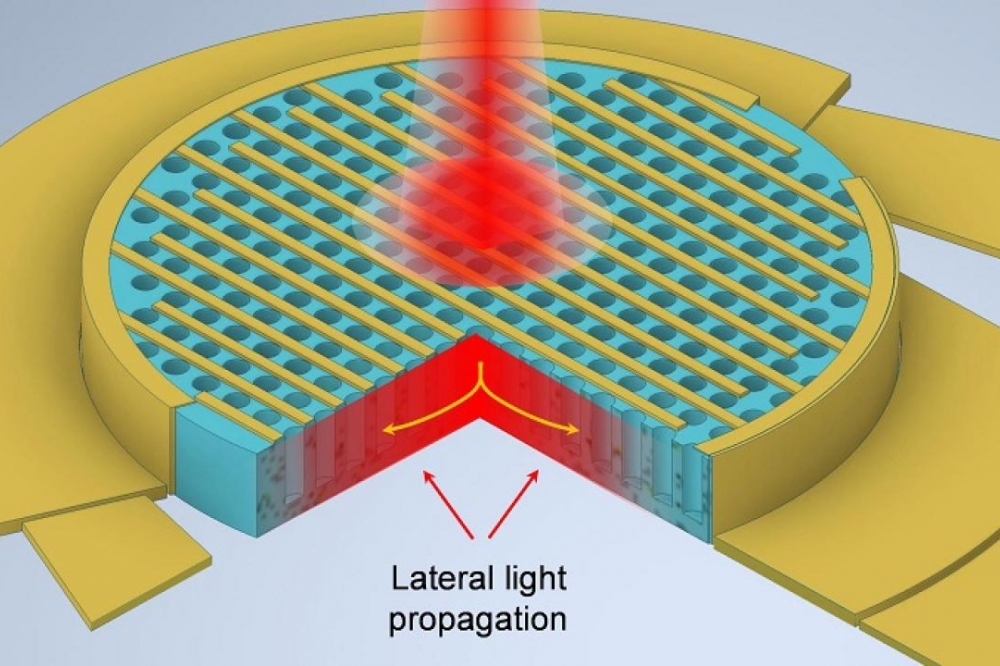
They created a micrometer-thick wafer of silicon with regular tiny holes in it. When infrared light hits the wafer, it is "trapped" by these structures, bends almost 90 degrees and travels sideways through the wafer, increasing contact with the semiconductor and enhancing the absorption of near infrared photons.

Simulations by the team showed that this photon trapping increases absorption by several times over a plain silicon wafer and actually outperforms GaAs.

Because the approach is compatible with chip manufacturing technology, the team says it could enable a new generation of cheaper photoelectronic devices.

Reference

'Achieving higher photoabsorption than group III-V semiconductors in ultrafast thin silicon photodetectors with integrated photon-trapping surface structures' by Wayesh Qarony et al; Advanced Photonics Nexus, Vol. 2, Issue 5, 056001 (July 2023)

QD company Quantum Science expands into new facility
Innoscience files lawsuit against Infineon
Riber revenues up 5% to €41.2m
Forvia Hella to use CoolSiC for next generation charging
Photon Design to exhibit QD simulation tool
Ortel transfers CW laser fabrication to Canada
Luminus adds red and blue multi-mode Lasers
PseudolithIC raises $6M for heterogeneous chiplet tech
Mesa sidewall design improves HV DUV LEDs
IQE revenue to exceed expectations
'Game-changing' VCSEL system targets clinical imaging
German start-up secures finance for SiC processing tech
Macom signs preliminaries for CHIPS Act funding
IQE and Quintessent partner on QD lasers for AI
EU funds perovskite tandems for fuel-free space propulsion
EU to invest €3m in GeSi quantum project
Transforming the current density of AlN Schottky barrier diodes
Turbocharging the GaN MOSFET with a HfO₂ gate
Wolfspeed launches Gen 4 SiC MOSFET technology
Report predicts high growth for UK's North East
Element Six unveils Cu-diamond composite
SemiQ launches hi-rel 1700V SiC MOSFETs
Lynred to exhibit Eyesential SWIR sensor for machine vision
Thorlabs buys VCSEL firm Praevium Research
Advancing tuneable InP lasers on a heterogeneous platform
P-GaN gate HEMTs have record threshold voltage
Guerrilla RF releases GaN power amplifier dice
Narrow-linewidth DFB lasers now at 405 and 488nm
Researchers develop tech for future fast-charging stations
Vermont GaN Tech Hub awarded nearly $24M
Onsemi completes buy-out of Qorvo SiC JFET business
Quantum Science announces Innovate UK funding
×
Search the news archive

To close this popup you can press escape or click the close icon.
Logo
x
Logo
×
Register - Step 1

You may choose to subscribe to the Compound Semiconductor Magazine, the Compound Semiconductor Newsletter, or both. You may also request additional information if required, before submitting your application.


Please subscribe me to:


You chose the industry type of "Other"

Please enter the industry that you work in:
 
x
Adblocker Detected
Please consider unblocking adverts on this website