
A new insight into non-radiative mechanisms
A trap-assisted process is behind defect-related losses in shorter wavelength GaN-based LEDs
One of the great mysteries of the LED is this: how do defects impact efficiency at ever shorter wavelengths? For many decades, it’s been common knowledge that LEDs emitting in the red and green are held back by a non-radiative recombination process located at defects and involving multi-phonon emission. But as this process exponentially decreases with bandgap, what is the defect-related mechanism that matters for blue and UV emitters?
Offering an answer to this intriguing question is a team of computational scientists at the University of California, Santa Barbara, led by Chris Van de Walle.
“Our newly developed methodology reveals that the trap-assisted Auger-Meitner effect can produce loss rates that are orders of magnitude greater than the mechanism based on multi-phonon emission alone, thus resolving the puzzle of how defects can cause loss in materials with wide bandgaps,” remarks Van de Walle.
This new loss mechanism is a cousin of what has often been referred to as the Auger process, reported by Pierre Auger in 1923, but also described in 1922 by Lise Meitner, a female physicist with many accomplishments who is only just starting to get the recognition she deserves. Accepted by many as the cause of LED droop, the Auger-Meitner process involves an electron combining with a hole to promote a second electron or hole to a higher energy state. Meanwhile, the related trap-assisted Auger-Meitner process, which the UCSB team has just identified as playing a key role in short-wavelength LEDs, involves the localisation of an electron or hole at a defect or impurity.
As extended defects, such as threading dislocations, are present in high densities in GaN-based LEDs, they seem to have little direct impact on the internal quantum efficiency of these devices. Thus, in order to increase device efficiency, there’s a need to focus on point defects, such as native defects or impurities, which are the class of defects considered by Van de Walle and his colleagues.
This team considered calcium impurities in their calculations. Calcium has been identified as an impurity in GaN LEDs grown by MBE, with the interloper introduced during wafer polishing. During growth by MBE, calcium appears to ride the surface until the deposition of the InGaN layer. However, this impurity does not seem to hamper LEDs grown by MOCVD, either because the different epitaxial conditions prevent calcium from riding the surface, or because it is caught in the InGaN layer beneath the active region.
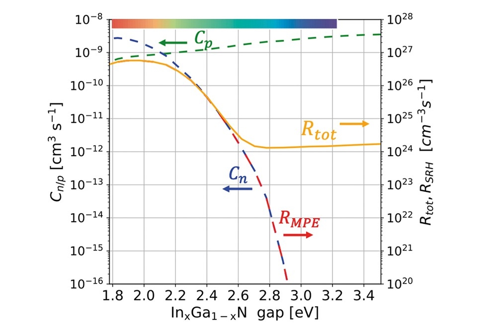
According to the team’s calculations, for a calcium impurity in GaN, defect-assisted recombination with the trap-assisted Auger-Meitner process is eleven orders of magnitude faster than recombination based on multi-phonon emission alone (see Figure).
At high current densities, the bulk Auger-Meitner process dominates, because this scales with the third power of the carrier density. But at a more modest carrier density, trap-assisted recombination is the most significant loss mechanism.
While some researchers may be tempted to add a non-radiative ‘B’ term to the ABC model that describes LED behaviour, Van de Walle warns that this is an over-simplification. “To fully describe nonradiative recombination at a trap, one needs to include both electron capture and hole capture. The most common scenario will be that one of these capture processes happens by trap-assisted Auger-Meitner, and the other still happens by multi-phonon emission.” Consequently, both a linear and a quadratic contribution are at play.
Van de Walle and his co-workers are now building on this work, by re-examining candidate defects and impurities that may be responsible for efficiency loss in wider-bandgap materials, but were previously dismissed because rates based on multi-phonon emission alone were too low. In addition, the researchers are investigating trap-assisted Auger-Meitner processes where the trap has more than one bound state. “Again, when only multi-phonon emission is considered, such defects show low nonradiative recombination rates, and we are curious to examine whether including trap-assisted Auger-Meitner changes this,” explains Van de Walle.
Picture caption: The multi-phonon emission process, denoted RMPE, cannot account for defect-related losses in short-wavelength LEDs. To explain this loss, trap-assisted Auger-Meitner processes must be included, as they are in RTOT.
Reference
Zhao. et al. Phys. Rev. Lett. 131 056402 (2023)


