The power of pseudomorphic nitrides
Pseudomorphic AlGaN/AlN promises to enhance the performance of UVC lasers, far-UVC emitters and high-power solid-state devices.
BY LEO SCHOWALTER FROM NAGOYA UNIVERSITY AND LIT THINKING AND MAKI KUSHIMOTO, ZIYI ZHANG, AKIRA YOSHIKAWA AND HIROSHI AMANO FROM NAGOYA UNIVERSITY
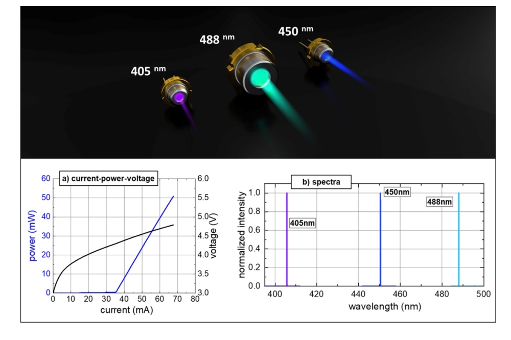
Recently, and for good reason, our community has been showing much interest in ultrawide bandgap semiconductors. Part of their appeal is their potential to create optoelectronic devices emitting in the UVC, a spectral domain associated with wavelengths below 280 nm (see Figure 1). But in addition, this class of semiconductors is a strong candidate for creating higher performance, high-power RF devices, and for increasing the power density and performance of power devices and power switches.
Figure 1. Nagoya University, working in partnership with Asahi Kasei/Crystal IS, has demonstrated the first UVC laser diodes
Unfortunately, ultrawide bandgap semiconductors are challenging for the very reasons that make them attractive. It’s the norm that very large bandgaps go hand-in-hand with very strong chemical bonds, leading to very high temperatures for crystal growth. Likewise, the large bandgaps hamper controlled doping of p-type and n-type carriers.
This is so severe that in the not so distant past, what we now call ultrawide bandgap semiconductors were listed as insulators! And even now, aside from a few special cases, it is incredibly challenging to realise reliable hole and electron conductivity in these materials.
One example of an ultrawide bandgap semiconductor is high-aluminium-content Al1-xGaxN. When the aluminium content in this alloy exceeds about 50 percent – that is, when the value of x is less than 0.5 – its bandgap monotonically increases with aluminium concentration from about 4.4 eV to 6.1 eV, when pure AlN is reached.
Figure 2. Nagoya University, working in partnership with Asahi Kasei/Crystal IS, has demonstrated the first UVC laser diodes.
Related to high-aluminium-content Al1-xGaxN is GaN, as well as the alloys of Al1-xGaxN and AlInGaN with bandgaps less than 3.5 eV. These materials have enjoyed much success, so it’s natural to try and builid on what has been accomplished by progressing the capabilities of ultrawide bandgap alloys of Al1-xGaxN with values for x that are less than 0.5.
While this may sound simple, the reality is far from that, with two major obstacles blocking the path to success. One is that the epitaxial growth of high-quality, high-aluminium-content AlGaN is relatively difficult on foreign substrates. It is much easier to undertake epitaxial growth on native bulk AlN, particularly at high aluminium concentrations, but progress has been held back by the lack of high-quality substrates.
The other major issue is the difficulty in doping high-aluminium-content AlGaN. Until recently, the most common approach to doping has been the addition of silicon, to produce n-type material. This dopant works quite well at aluminium concentrations below 85 percent and, very recently, researchers at Georgia Tech have even shown successful n-type doping of AlN. However, producing p-type doping is much more problematic.
Breaking new ground by overcoming both these issues is our team at Nagoya University, which has been working in partnership with Asahi Kasei/Crystal IS. Our recent demonstration of UVC laser diodes highlights that we have established a clear path past these issues that can unlock the door to allowing high-aluminium-content AlGaN to play a much bigger role in ultrawide bandgap device applications (see Figure 1).
Our work is an important milestone in the development of the UVC laser diode, a device that has been intensely pursued for more than 20 years. The commercialisation of a low-cost laser diode in the UVC will revolutionise portable, cost-effective chemical and particle detectors, medical instrumentation, and surface monitoring and machining. All these applications draw on short-wavelength high-energy photons and their very short absorption length in most materials.
However, despite the great demand for such a source that inspired numerous development efforts, the shortest wavelength laser diode developed prior to our successful demonstration of a 271 nm laser diode in October 2019 only reached down to a wavelength of 315 nm (see Figure 2).
There are two keys to our success. One is the availability of pseudomorphic Al1-xGaxN on high-quality AlN substrates, and the other is the use of distributed polarisation doping. With this form of doping it’s possible to realise low-resistivity hole injection without the use of impurity doping in the p-type laser cladding layer.
Figure 3. In high-aluminium-content AlGaN, misfit dislocations may form along the interface.
What is pseudomorphic AlGaN/AlN?
Due to progress in bulk crystal growth of AlN, several companies, including Crystal IS, are now supplying substrates. This foundation for epi-growth comes from slicing material from AlN crystals with very low defect densities.
During the growth of nitride semiconductor heterostructures, one defect that arises in the epilayers is the so-called threading dislocation. High densities of this type of dislocation tend to arise during growth on foreign substrates, such as sapphire, SiC or silicon, due to lattice mismatch. As these threading dislocations degrade device performance, the nitride community has devoted much effort to reducing their density, as well as mitigating the impact that they have on devices. But despite all this work, it still takes a great deal of care to bring the threading dislocations in high-aluminium-content AlGaN below 108 cm-2, leading to a high cost.
The good news is that 2-inch AlN substrates with threading dislocation densities of less than 103 cm-2 are now available from a couple of suppliers, and there are more producers on the horizon. When the surfaces of these substrates are properly prepared (most typically, the Al-polar c-face), AlN homoepitaxy with threading dislocation densities below 104 cm-2 are routinely produced.
Crucially, AlN substrates can also provide the foundation for AlGaN alloys with very low threading dislocation densities. Since the crystal structure of GaN, AlN and related alloys is identical, one would hope that a well-prepared surface of native AlN would act as a good template for the growth of all AlGaN alloys. Unfortunately there is a significant lattice mismatch between bulk GaN and AlN – it is as high as 2.4 percent. Thus, if GaN is grown on AlN using the c-face crystal surface as a template, the epitaxial GaN layer is compressively strained in the c-plane by 2.4 percent. This results in an enormous strain energy, increasing linearly with the thickness of the GaN layer. Eventually, this strain has to be relieved in some way.
As epitaxial growers are well aware, there are a number of mechanisms for strain relief, including forming islands and roughening the surface. However, the mechanism that is most significant for high-aluminium-content AlGaN is the formation of a misfit dislocation along the interface (see Figure 3). As shown in that figure, an edge misfit dislocation forms when a plane of atoms is skipped along the interface, leading to a reduction in the compression of the GaN epitaxial layer that fits onto the underlying AlN lattice.
Figure 4. In this pseudomorphic UVC laser diode the top edge of the
etched mesa is no longer strained while the bottom corner of the mesa
remains fully strained.
At the core of the misfit dislocation is a row of atoms with dangling bonds. That’s not the only concern, however, as there is an inhomogeneous strain field surrounding the misfit dislocation. Together, they result in a ‘core energy’ associated with each misfit dislocation and additional strain energy that arises from non-uniformity. For more than half a century it has been known that the extra energy introduced by an array of misfit dislocations can be balanced by a reduced elastic strain energy that results from the misfit array once the strained epitaxial layer exceeds a critical thickness.
If the thickness of the layer is below the critical thickness, the epitaxial film is in a lower energy state and pseudomorphically strained to exactly match the lattice parameter of the underlying substrate. For the growth of GaN on AlN, the critical thickness is only a few nanometres. Using Vegard’s law, it is possible to estimate the lattice mismatch between AlGaN and AlN. This approach, involving linear interpolation, determines that for Al0.6Ga0.4N the lattice mismatch is still almost 1 percent – and roughly speaking, the critical thickness is only increased by a factor of 2.5, far short of what’s needed for most device structures.
Fortunately, the reality is better than these predictions. Back in 2009 our colleagues at Crystal IS showed that it is possible to grow a 0.5 µm-thick layer of Al0.6Ga0.4N pseudomorphically on the c-face of an AlN substrate. Since then, even thicker pseudomorphic layers have been demonstrated for layers of AlGaN with a higher aluminium content.
While this was a very surprising result at the time, it can be explained. While the strain energy in the epitaxial layer would be reduced by forming a misfit network of dislocations, there are no easy glide planes. That matters because without these glide planes, dislocations, which form on the surface of the epitaxial layer, cannot be pushed down to the AlGaN /AlN interface to relieve the strain. As a result, the strain energy in the epitaxial layer can become much, much larger than equilibrium models predict.
Figure 5. Severe strain inhomogeneity can generate very large shear
stresses at the corner of the mesa that drive misfit dislocations in
from the sides of the structures.
P-type polarisation doping
A rather special feature of nitride semiconductors is that it is possible, at least in principle, to create regions of n-type or p-type carriers by simply changing the alloy composition at an interface. Exploiting this phenomenon are the high-performance GaN HEMTs that are serving in the RF and power industries. Their success is built on efforts in the 1990s, which showed that a two-dimensional electron gas can be created at the interface between GaN and AlGaN. This gas, formed without doping with any extrinsic impurity, results from the growth in the metal-polar direction of a layer of AlGaN on top of GaN.
Note that this is a very different state of affairs from that found in cubic semiconductors. For instance, to create a two-dimensional electron gas at the interface of GaAs and AlGaAs, an n-type impurity dopant, typically silicon, must be introduced in the wider bandgap AlGaAs epitaxial layer.
With the nitrides, the creation of a two-dimensional electron gas at an interface is not limited to the pairing of AlGaN and GaN. This gas arises at any interface where the aluminium concentration of AlGaN is stepped up when growing on a metal-polar c-face substrate, so long as the defect density is not too high. What’s more – as demonstrated by researchers at the University of California, Santa Barbara, back in 2002 – even grading an epitaxial layer from a lower to a higher aluminium concentration yields a distributed electron gas without extrinsic impurity doping. Note that this type of doping is referred to as distributed polarisation doping.
What about grading in the opposite direction – that is, from a high to a low aluminium concentration, when growing on a metal-polar c-face substrate? This was predicted to produce a distributed p-type semiconductor without the use of any extrinsic impurity doping. However, experimental demonstration did not immediately follow, although an increase in the hole concentration was observed in extrinsically doped p-type material, typically doped with magnesium, over what would be expected from just extrinsic doping. The barrier to forming a hole gas without extrinsic doping in this earlier work appears to have been a high density of defects. These defects trap holes, which must be saturated before the effect
of distributed polarisation doping can be observed.
Against this backdrop, our demonstration of the first UVC laser diode has to be viewed as incredibly encouraging. To produce this device, we realised high hole conductivity in a distributed polarisation- doped p-side cladding layer. Here there is no use of extrinsic dopants, and the aluminium concentration is increased to 63 percent. Another key to this breakthrough in laser performance is the very low density of threading dislocations that results from pseudomorphic growth. We view our development of pseudomorphic AlGaN /AlN as crucial to the realisation of distributed polarisation doping in our devices.
A price to be paid
It’s rare that any technology is free from downsides. In that respect, pseudomorphic epitaxial growth conforms to the norm, with its many benefits having to be weighed against a couple of problems that need addressing.
One weakness is that while the thickness of the pseudomorphic layers can be remarkably high, it is still finite. While it is possible for epitaxial growers to modify their process conditions and exceed the limits predicted by equilibrium models by at least three orders of magnitude, even then the constraints are rather limiting, especially when the gallium concentration of some of the epitaxial layers is increased. In general, there will be a roughening of the epitaxial layer once the pseudomorphic limit is exceeded. As this limit depends on the epitaxial conditions, a formal model of the limit is yet to be developed. This hampers efforts to account for the impact of the epitaxial process on the quality of the heterostructure, which influences considerations associated with device design. The other limitation is not so obvious. Producing devices involves etching into highly strained epitaxial layers, which breaks the two-dimensional symmetry. Rather than being uniformly compressed to fit onto the underlying AlN lattice, all local three-dimensional features have strains that are not uniform in the plane, with the non-uniformity giving rise to locally high stresses.
This high degree of local stress occurs at the corners of a mesa created by etching. Consider, for example, Figure 4, illustrating the etching of pseudomorphic layers of a UVC laser diode. In this particular case, the top edge of the etched mesa is no longer strained while the bottom corner of the mesa remains fully strained. This severe strain inhomogeneity is certainly cause for concern, because it generates very large shear stresses at the corner of the mesa that can drive misfit dislocations in from the sides of the structures – in this case, the mesa walls (this is illustrated in Figure 5). If these dislocations reach the active region of the device, including regions of high current density, they will degrade device performance.
We have observed this mechanical instability in the etched epitaxial layers when fabricating laser diode structures. Our device designers wanted to put the n- and p-contacts as close to one another as possible to reduce the laser’s electrical resistance. This must be minimised to trim resultant Joule heating, which threatens to hike the threshold current required for lasing. To position the n- and p-contacts as close to one another as possible, we etched the vertical wall mesas and positioned our p-type metallisation that sits at the top of the mesa and our n-metallisation that’s located at the bottom of the mesa as close to the mesa wall as possible. Unfortunately, the vertical mesa walls resulted in the injection of misfit dislocations into the device structure (shown schematically in Figure 4) during thermal annealing of the metal contacts.
Compounding our problems, the high temperatures that we employed for annealing reduced the Peierls stress required for dislocation motion, causing AlGaN to plastically deform. The dislocations injected from the mesa edge, visible in a plane-view transmission electron microscopy image (see Figure 6), created an effective dead region near the sidewalls and forced the p-contacts to be moved further from the sidewalls to avoid this dislocated region. Moving the p-contact away from the mesa wall has pros and cons. It improves the laser performance, by reducing the threshold current and increasing device lifetime, but it also increases resistivity – this led to self-heating that prevented room-temperature CW operation, because the threshold current increased too rapidly.
Our solution is to engineer the side walls of the etched mesa to ensure a reduction in the build-up of shear stress. By introducing a sloped mesa wall, we significantly reduce the maximum shear stress present in the etched structure (see Figure 5). With this new architecture, annealing of our device does not induce misfit dislocations, and our p-metal can be placed much closer to the mesa edge, enabling a reduction in the resistance of the laser diode.
The key point here is that it is possible to engineer the stress in the sidewalls in a manner that avoids exceeding the minimum shear stress that will result in misfit dislocation injection, even at elevated temperatures. This is a major breakthrough for the practical application of pseudomorphic epitaxial structures.
Figure 6. Dislocations injected from the mesa edge are visible by various forms of electron microscopy.
Where next?
As well as UVC laser diodes, there are other exciting opportunities for ultrawide bandgap semiconductors, which can be used to solve several of society’s problems. For instance, this class of materials can be used to develop solid-state sources of far-UVC radiation, emitting below 235 nm – this corresponds to a photon energy of more than 5.3 eV. At such short wavelengths, radiation is so strongly absorbed by protein and other organic molecules that it is unable to penetrate the skin or the surface of the eye, preventing damage to the DNA in living cells. Meanwhile, viruses and bacterial pathogens have no such protection, and will be neutralised by relatively small exposures to such radiation. Thanks to this, it is possible to safely disinfect rooms where humans are present.
It’s worth noting that gas sources of far-UVC radiation are available. However, as they are rather inefficient and expensive, far-UVC LEDs promise to be an attractive alternative, offering a much lower cost and superior robustness. Within the family of ultrawide bandgap semiconductors, the pseudomorphic high-aluminium-content AlGaN /AlN system offers potential: it has a bandgap that approaches 6.1 eV, and can form p-type material with distributed polarisation doping.
Additional opportunities for ultrawide bandgap semiconductors are associated with electrical grids, which need to evolve to handle future demands, resulting from distributed power generation and storage. As we shift to a world with a lower carbon footprint, we will move away from the centralised mega-power generators, which depend on fossil fuels, to many sources of relatively small, renewable power generation. These greener alternatives are often neither continuous nor ‘on-demand’, necessitating a hike in energy storage capability. What’s required is a ‘smart-grid’ that handles power regulation without having to put up power substations in every square block – at least, not the large, unsightly and vulnerable kind currently used.
Amongst the ultrawide bandgap semiconductors that can help in this particular endeavour is AlN, which has the potential to enable the development of power control systems that handle much higher power densities reliably, while shrinking the volume to enable a substation in a box. With any ultrawide bandgap semiconductor there have always been challenges in realising p-type and n-type carriers; but distributed polarisation doping presents an extremely useful new tool to accomplishing this for the high-power device designer, who also benefits from pseudomorphic growth, key to realising the low defect densities that ensure long-term reliable operation.
What is abundantly clear is that the potential for pseudomorphic, high-aluminium-content AlGaN/GaN is very high.
Further reading
J.Y. Tsao et al. “Ultrawide-Bandgap Semiconductors: Research Opportunities and Challenges” Adv. Electron.Mater. 4 1600501 (2018)
Jena et al. ”Realization of wide electron slabs by polarization bulk doping in graded III–V nitride semiconductor alloys,” Appl. Phys. Lett. 81 4395 (2002)
J.R. Grandusky et al. “Pseudomorphic growth of thick n-type AlxGa1xN layers on low-defect density bulk AlN substrates for UV LED applications,” J. Crystal Growth 311 2864 (2009)
M. Kushimoto et al. “Local stress control to suppress dislocation generation for pseudomorphically grown AlGaN UV-C laser diodes” Appl. Phys. Lett. 121 222101 (2022)
“New Type of Ultraviolet Light Makes Indoor Air as Safe as Outdoors,” https://www.cuimc.columbia.edu/news/new-type-ultraviolet-light-makes-indoor-air-safe-outdoors (2022)


