
Advancing amber microLEDs
Passivated emitters with capped quantum wells set a new benchmark for the efficiency of long-wavelength GaN-based LEDs
A team from the University of California, Santa Barbara, is claiming to have made major strides towards the development of ultra-small, highly-efficient red LEDs.
The researcher’s InGaN-based microLEDs, which have dimensions of 10 µm by 10 mm and a peak emission wavelength of 601 nm, produce a peak external quantum efficiency of 5.5 percent and a maximum wall-plug efficiency of 3.2 perceµt. What’s also encouraging is that the efficiency droop of these devices scales in a very similar manner to that of comparable devices with dimensions of 100 µm by 100 µm.
This work is an important step towards the development of efficient microLEDs emitting in the red, green and blue. Augmented reality and virtual reality displays need these three sources, each with dimensions below 10 µm, to produce high-quality colour images.
One candidate material for the red microLED is AlInGaP. However, this alloy that is employed in traditional red LEDs has a high surface recombination velocity, causing efficiency to plummet as device dimensions shrink. While red AlInGaP LEDs with a size of around 0.1 mm2 have an external quantum efficiency of around 20 percent, this falls to just 3 percent for variants with dimensions of 10 µm.
Much innovation has been directed at improving the performance of red-emitting GaN-based LEDs, which are far less sensitive to scaling than their AlInGaP siblings when proper sidewall passivation and treatment is employed. However, these nitride-based emitters are held back by two significant issues: a strong internal electric field, which impairs radiative recombination; and a significant lattice mismatch between the InGaN quantum wells and GaN layers, giving rise to a high density of light-quenching defects.
Novel approaches to improving the performance of red InGaN LEDs include the UCSB group’s growth of the epistructure on a nano-porous GaN substrate. In 2021, they reported 6 µm microLEDs with an external quantum efficiency of 0.2 percent that incorporated this technology. That year, using pattern sapphire, a team from King Abdullah University of Science and Technology announced in external quantum efficiency of 0.56 percent in 47 µm red microLEDs, while partnership between researchers at the University of Grenoble-Alpes and Soitec reported an external quantum efficiency of 0.14 percent for 47 µm amber microLEDs on a relaxed pseudo-substrate. More impressive results have come from a collaboration led by National Yang Ming Chiao Tung University: last year that team reported a peak external quantum efficiency of 2.91 percent for amber LEDs, but even this is overshadowed by the latest claims from UCSB.
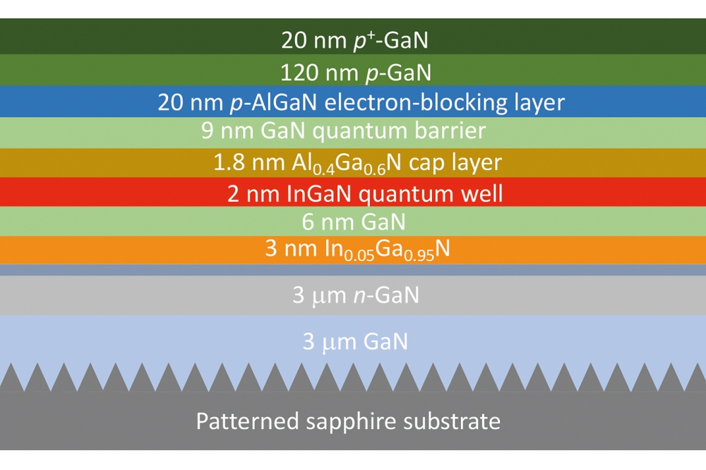
Their latest devices have been produced by loading patterned sapphire substrates into an MOCVD chamber and depositing an epitaxial stack featuring a 6-period active region with InGaN wells, AlGaN cap layers and GaN barriers (see figure above for details). Fabrication of devices began with the deposition of a 110 nm-thick layer of ITO on these epiwafers, followed by the formation of mesas via stepper lithography and reactive-ion etching. After sidewall treatment with potassium hydroxide and the addition of a reflective dielectric stack by ion-beam deposition, atomic layer deposition of a 30 nm-thick layer of SiO2 ensured sidewall passivation, before evaporation added metal contacts.
Measurements of these microLEDs reveal a turn-on voltage of 2.6 V at 1 A cm-2 and a reverse current of just a nanoamp at -3 V. According to the team, these findings imply good quality for the epitaxial materials, the etching process and the passivation.
Peak electrical efficiency at 1 A cm-2 is 0.83, exceeding the group’s previous value for red InGaN microLEDs. This improvement is attributed to optimisation of the active region and sidewall chemical treatment. As the drive current increases from 0.5 A cm-2 to 80 A cm-2, the peak emission shortens from 614 nm to 593 nm. This shift, stemming from screening of the electric field and band filling of localised states, is claimed to be smaller than that for most red and amber microLEDs.
The researchers believe that their work paves the way for the realisation of highly efficient red microLEDs with sizes down to 1 µm and below.
Picture caption: The epistructure of InGaN microLEDs produced by UCSB.
Reference
P. Li et al. Appl. Phys. Express 16 064002 (2023)


