
Better FETs with bulk AlN
A native foundation equips nitride FETs with a higher drain current and lower thermal impedance
Engineers from the University of South Carolina are claiming to have raised the bar for the performance of nitride FETs with an aluminium-rich AlGaN channel.
The team’s devices, grown on bulk AlN, are said to break the record for the Baliga’s figure-of-merit for this class of transistor. For that metric – the square of the breakdown voltage, divided by the specific on-resistance – the researcher’s FETs have a value of 460 MW cm-2.
According to these engineers, their devices could improve the performance of nitride-based transistors in consumer chargers and next-generation electric vehicles. Advances have come from addressing thermal limitations with AlN substrates, which are blessed with a high thermal conductivity.
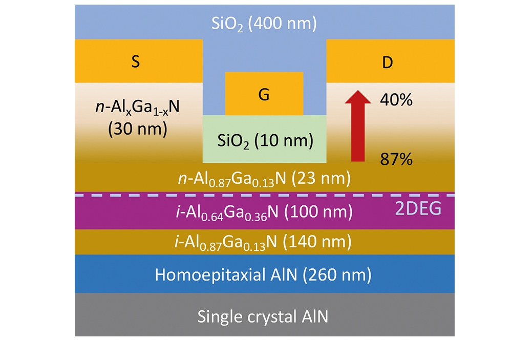
Metal-oxide-semiconductor FETs were fabricated on a 400 mm-thick single-crystal AlN substrate grown by physical vapour transport and purchased from HexaTech. Engineers loaded this substrate into a low-pressure MOCVD reactor and deposited an epitaxial stack consisting of a 260 nm-thick AlN layer, a 140 nm-thick Al0.87Ga0.13N back-barrier, a 100 nm-thick Al0.64Ga0.36N channel, a 23-nm thick n-type Al0.87Ga0.13N barrier, and a 30 nm-thick graded AlGaN layer that’s silicon-doped and designed to support the formation of ohmic contacts.
Device fabrication began by using reactive-ion etching to form a mesa. Electron-beam evaporation added source and drain contacts, which were annealed, before a second etching step removed the graded layer from the access region, prior to the introduction of a 10 nm-thick layer of SiO2 that serves as the gate oxide. After electron-beam evaporation added gate and probe pads, devices were embedded in a 400 nm-thick SiO2 film by plasma-enhanced CVD to relieve the surface electric field during breakdown measurements. To provide a control, identical structures were fabricated on an AlN template, formed by depositing a 3 µm-thick layer of AlN on sapphire.
Electrical measurements on FETs with a gate length of 1.8 µm, a gate-to-source distance of 1.2 µm, and a gate-to-drain distance of 2.64 µm, exhibited clear saturation and pinch-off. Peak currents of 610 mA mm-1 and 410 mA mm-1 were recorded for devices on the native substrate and template, respectively.
Thermal droop is seen in the FET with the sapphire foundation, but not in the variant built on AlN. The lack of droop is said to result from superior thermal management. Thermal impedance measurements reveal a value of 10 K mm W-1 for the device on AlN, and 31 K mm W-1 for that on sapphire.
The team attributes the far lower thermal impedance, which is supported by an 8-fold higher thermal conductivity for AlN than sapphire, to the higher value for the peak current.
Due to the presence of the SiO2 gate insulator, the team did not expect to see any difference in reverse leakage current between the two types of device. But leakage in the sapphire-based device is noticeably higher at positive gate voltages, a finding that is said to require further study.
The peak value for transconductance – the product of channel mobility and gate capacitance – hit 45 mS mm-1 in the FET on AlN, compared with 34 mS mm-1for the variant on sapphire. As the gate capacitance is similar in both devices, the superior transconductance in the device on the native foundation is thought to be associated with an inferior mobility, which gives rise to thermal droop.
At a gate-source voltage of -30 V, device breakdown is 959 V, leading to a ‘conservative’ estimate for Baliga’s figure-of-merit of 460 MW cm-2. It is argued that because the annealed contacts are unlikely to produce an isotropic in-plane two-dimensional electron gas, a reasonable upper bound for the figure of merit is more than 750 MW cm-2 – that’s claimed to be ten times higher than other results for FETs on AlN, and represents the state-of-the-art.
Picture caption: Fabricated on single-crystal AlN, the nitride FET produced at the University of South Carolina has a thermal impedance of just 10 K mm W-1.
Reference
A. Mamum et al. Appl. Phys. Express 16 061001 (2023)


