
EU project develops devices using MoS2, SiC and GaN
FLAG-ERA ETMOS project makes ultra-fast diodes and transistors using 2D materials and wide-bandgap semiconductors
SiC and group-III nitrides are playing a crucial role in energy-efficient power conversion, high-frequency electronics and optoelectronics. Now European researchers have come up with new devices by combining these wide bandgap semiconductors with 2D materials.
Part of the FLAG-ERA ETMOS project (Epitaxial Transition Metal dichalcogenides Onto wide bandgap hexagonal Semiconductors for advanced electronics), researchers from CNR-IMM (Italy), CNRS-CRHEA (France), IEE-SAS (Slovakia), MFA-EK (Hungary), and the University of Palermo (Italy) have developed MoS2/SiC and MoS2/GaN heterojunction diodes with excellent rectification properties. Tuneable current injection was achieved by tailoring the doping.
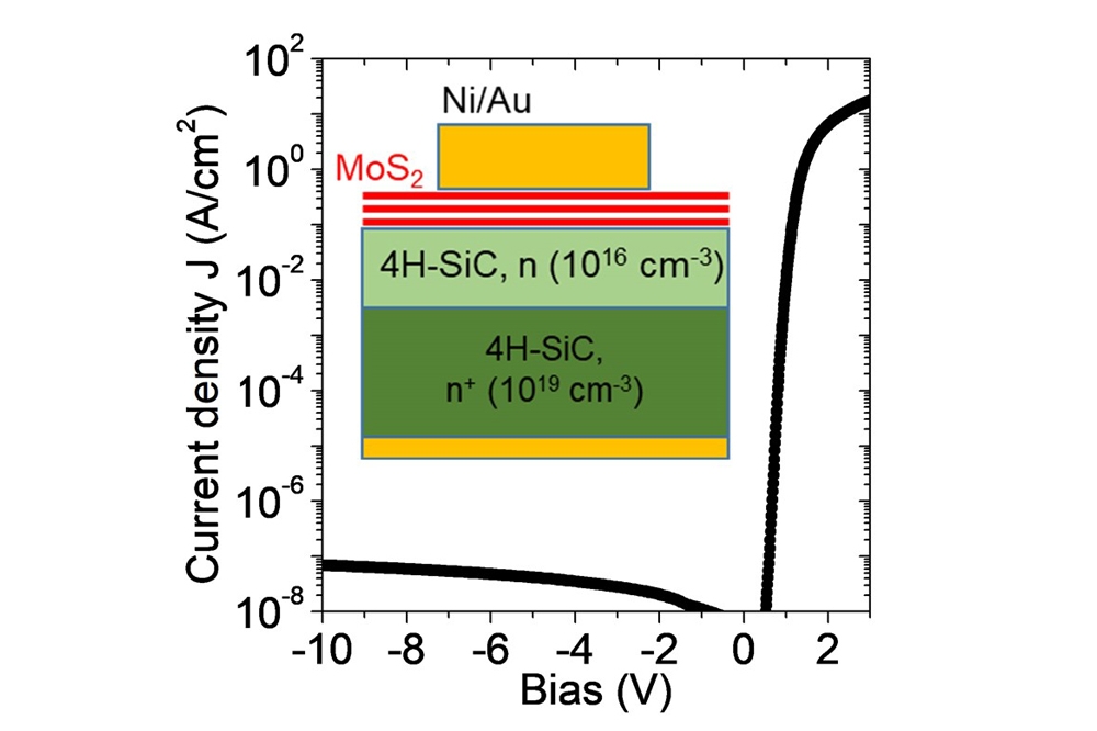
Pictured above is a graph showing the current density versus bias characteristic of a MoS2/4H-SiC heterojunction diode.
Given the high application potential of this research in the field of high-power and high frequency electronics, the Italian company STMicroelectronics came on board, resulting in two US patent applications, shared between CNR and STMicroelectronics, on ultra fast diodes and transistors based on the combination of MoS2 with SiC and GaN.
To build such structures, the team explored different methodologies, including single and double-step CVD, pulsed laser deposition (PLD), MBE and advanced exfoliation/transfer methods. The researchers also assessed various characterisation protocols, based on the combination of micro-Raman, atomic force microscopy (AFM/conductive-AFM) and atomic resolution transmission electron microscopes, to evaluate the number of layers, doping, strain of MoS2, and the current injection at MoS2 heterojunctions with SiC and GaN.
“The integration of 2D materials provides new functionalities to SiC and GaN, expanding the range of potential applications of these wide bandgap semiconductors. I expect that new market opportunities will be opened by this technology,” says CNR-IMM’s research director Filippo Giannazzo.


