
GaN: Going beyond fast charging
Navitas has introduced a range of GaNSafe ICs to expand its sales into electric vehicle, solar and data-centre markets.
BY RICHARD STEVENSON, EDITOR, CS MAGAZINE
In the fast charging of mobile devices GaN found its first killer application. But as is often the case with mass market adoption, phenomenal success has led to lower margins and ultimately commoditisation. So, for the makers of this class of device, efforts must now be directed at developing new products for new applications.
That’s the latest strategy of the US-based wide bandgap specialist Navitas Semiconductors, which unveiled its GaNSafe portfolio this September.
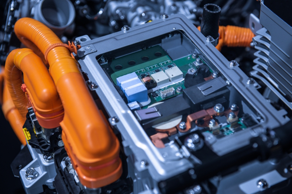
Strictly speaking, this fabless firm has also had success in a handful of other consumer applications, with its established range of GaN devices deployed to drive motors in washing machines, hairdryers and vacuum cleaners. “But there has been a glass ceiling into data centre, into solar and into electric vehicles,” says Stephen Oliver, Navitas’ VP of Corporate Marketing & Investor Relations. He told Compound Semiconductor that while the company’s previous products excel in efficiency, reliability and quality, they don't meet all the needs for lengthy operation at high powers. “The GaNsafe range breaks through, smashes that glass ceiling, and can now be taken seriously by customers in the high-power areas.”

Navitas’ GaNSafe ICs have unprecedented functionality.
There is a rich heritage behind the GaNSafe portfolio, which today has four parts, each designed to operate at 650 V and handle up to 800 V. Together spanning the delivery of electrical power between 1 kW and 22 kW, these packaged ICs that are based on Navitas’s fourth generation of GaN benefit from three rounds of about one-fifth die shrink compared with the debut range that came out in 2018. Over that intervening years the company has equipped the GaN IC with more features, such as lossless current sensing and 2 kV electrostatic discharge protection. The launch of GaNSafe includes the addition of short-circuit protection and a higher operating temperature.
To enable higher power operation, GaNsafe features refinements to both the IC and its packaging. The three key advances at the chip level are: the introduction of a Miller clamp; a more intelligent approach to handling short-circuits, as well as ensuring overcurrent protection; and an absence of overshoot and undershoot during switching.
Note that even a well-designed device, operating in an efficient manner, can run into problems by generating electromagnetic interference (EMI). But with GaNSafe it is possible to reduce any spikes in EMI via external programming.
“That means that the design team doesn't have to do another spin and cross their fingers and hope they found the thing that's making the spike,” enthuses Oliver. “You can tune it in in real time.”
Perfecting the package
Innovation is also seen in the 10 mm by 10 mm package, referred to as TOLL – Transistor Outline Lead-Less. Despite the tremendous functionality of the GaNSafe IC, just four external connections are used, allowing leads to be fused together. This creates what is essentially a solid lump of copper, aiding thermal performance, a particular valuable asset in solar systems that undergo wide variations in temperature every day.
Navitas has also ‘keyed’ some of the pins in its GaNSafe design, creating a ridge metal surrounded by plastic. It’s a design that ensures a tough joint, aiding the mechanical integrity of the product.
Another strength of GaNSafe is that it is better at handling humidity and preventing liquid ingress. “It's a longer path for any humidity to get into the package and destroy it,” explains Oliver.
Since the start of this year, about 40 of Navitas’ customers have been working with products from the GaNSafe portfolio. These firms include: Enphase, a producer of power inverters for the Solar Industry; and Geely, a maker of power systems for the electric vehicle (EV) market that supplies its products to Volvo’s EV off-shoot Polestar, as well as Proton and Lotus.
To help succeed in new markets, Navitas has set up design centres for a data centre power team and an electric vehicle team. Both are staffed with a mix of talent, including experts in devices and those with real-world system knowledge, gained in previous roles outside Navitas. These design teams offer tremendous support to customers, including details for the full bill of materials, circuit diagrams, a PCB layout, and results of tests of EMI, thermal characteristics and efficiency.
One reason why these design teams are needed is that some of the companies that they work with are only just starting to move away from silicon power devices.
“With GaN, we are asking people to go from 50 kilohertz switching for the system to 500 kilohertz-to-a-megahertz, which means that they can't use the same control chip from their favourite provider that they've used for the last 20 years,” says Oliver. Navitas can help in this instance, by advising customers about suitable replacement components.

Through sourcing and ‘keying’, GaNSafe ICs deliver a superior thermal performance to their predecessors.
Minimising manufacturing costs
To produce its GaN devices, Navitas partners with an undisclosed packaging partner and the world’s biggest foundry, TSMC. Some may question this approach, claiming that it’s hard to develop breakthrough technologies with external fabs, while warning that it is risky to depend on partners when there’s a need to ramp volume. But Oliver questions both these views, seeing the situation very differently.
“Circuit development has nothing to do with the fab,” counters Oliver “It's all about good engineers sitting around the table, having good ideas and making it happen.”
And while he agrees that it’s vital to have capacity, he argues that the crucial question is whether it is economical to have that capacity. He sees no sense in spending billions on new fabs – as Wolfspeed and Infineon are doing – and points out that there is no need to buy new equipment to make state-of-the-art GaN devices. At TSMC, Navitas’ latest ICs are produced on 500 nm equipment around 30 years old.
Fabs with this level of capability are very common, with plenty in the US running silicon products on 6-inch and 8-inch lines at low margins. Retrofitted with a handful of tools, they can produce GaN ICs within a year, a move that is welcome, thanks to the higher margins.
With access to capacity clearly not an issue, and GaN ICs gaining traction in new markets, Navitas looks assured of a successful future.


