Enabling coherent optical communication with InP PICs

Combining InP PICs with state-of-the-art silicon CMOS process nodes creates an incredibly efficient coherent technology with exceptional date rates.
BY PAUL MOMTAHAN FROM INFINERA
Emerging in the late 2000s, coherent optical technology has revolutionised optical transport over long-haul, submarine, data centre interconnect and metro networks. Prior to the introduction of this technology, optical communication had a more primitive format, involving simply on/off modulation. Commonly referred to as intensity-modulation direct detection, this previous standard involved transmitting one bit per symbol for each wavelength, initially at 2.5 Gbit/s and then 10 Gbit/s.
The migration to coherent modulation has underpinned tremendous increases in wavelength speed, spectral efficiency and fibre capacity. Wavelength speed shot up from 10 Gbit/s to 100 Gbit/s, then to 200 Gbit/s, 400 Gbit/s, 600 Gbit/s, and most recently 800 Gb/s. And that’s certainly not the end of the line, with even higher-speed coherent engines poised to hit the market, including the 1.2 Tbit/s ICE7 from our company, Infinera.
Fibre capacity is benefitting from the increase in wavelength speed. For the extended C-band, having a bandwidth of 4.8 THz, fibre capacity has evolved from 960 Gbit/s (e.g., 96 x 10 Gbit/s) to 9.6 Tbit/s (e.g., 96 x 100 Gbit/s) and most recently to more than 40 Tbit/s (e.g., 53 x 800 Gbit/s).
There are also other advantages that come from the introduction of coherent technology. One is a simpler optical infrastructure, as there is no longer a need for a carefully planned dispersion compensation module placement. Another is that coherent technology can now provide data rates of 400 Gbit/s in compact pluggable form factors, such as QSFP-DD, that can be plugged directly into non-transport host devices, such as routers. What’s more, power consumption is lower than ever – it fell from approximately 5 W/G with 10 Gbit/s to around 2 W/G with the first generation of 100 Gbit/s coherent, and is now around just 0.05 W/G with today’s 400 Gbit/s pluggables. So how do these miraculous devices work, and what role does InP play in them?
Figure 1: Coherent optical engine high-level building blocks
Inside a coherent optical engine
To understand the role of InP, one must understand the building blocks and functions inside a coherent optical engine (see Figure 1). In these engines there are three basic, high-level building blocks: a digital ASIC/DSP, analogue electronics, and photonics. Often the analogue electronics and photonics are packaged together as a transmit-receive optical sub-assembly. Together with the RF interconnects and packaging, these three basic building blocks constitute a coherent optical engine. Note, though, that each of these blocks actually consists of multiple functions.
Leveraging state-of-the-art silicon CMOS process nodes – such as 7 nm, but evolving to 5 nm, then 3 nm and beyond – in the digital ASIC, often referred to as simply ‘the DSP’, there are digital signal processing (DSP) functions for the receive and transmit directions and the digital-to-analogue converter (DAC) and the analogue-to-digital converter (ADC). In addition, digital ASICs tend to incorporate other functions, such as forward-error correction, framing, multiplexing, encryption and performance monitoring.
In the transmit direction, drivers take the low voltages from the DAC and convert them to higher voltages required by the modulator. Meanwhile, in the receive direction, the transimpedance amplifiers take the currents from the photodetectors and convert them to the voltages required by the ADC.
The analogue electronics building block, typically packaged as a single ASIC, is made from a material other than the CMOS silicon used for the digital ASIC. For example, in Infinera’s coherent engines, analogue ASICs are made from SiGe.
Inside the photonics
For the third building block, which provides photonics, the key transmit functions include the laser and the modulator. Generating light with the required frequency, the laser is always made from InP. Its emission is coupled into the modulator, which encodes data by changing the phase and amplitude of the light, using an electric field to alter the refractive index of the material the light passes through.
A coherent modulator leverages four Mach-Zehnder modulators. Each splits the light into two arms, with phase changes either taking place in one arm, or more typically both arms. When the light is subsequently combined, interference controls the resulting amplitude. As a pair of phase-shifted Mach-Zehnder modulators are needed to control amplitude and phase, four are required for coherent transmission, due to the two polarisations.
There are a number of other components inside a coherent modulator. They include splitters, combiners, phase shifters, a polarisation rotator and a polarisation beam combiner. In addition, some coherent engines include an amplifier in the transmit direction to boost the wavelength power. Depending on the type of amplifier, a tuneable optical filter might also be included, to minimise this amplifier’s out-of-band noise.
The receive direction contains passive photonics and photodetectors. The passives include: a polarisation beam splitter, which separates the two polarisations of the coherent signal; and a pair of 90° hybrids, which extract the phase and amplitude from each polarisation, in the form of the in-phase and quadrature components. The role of the photodetectors is to detect light and convert it to electrical current. There is also a laser in this part of the photonics building block, employed to help extract phase information from the received modulated wavelength. In many devices, this laser is also used in the transmit section. However, in devices such as Infinera’s ICE6, separate lasers are deployed for transmit and receive.
Photonic integrated circuits
When coherent optical engines were in their infancy, their photonics building blocks were constructed from hundreds of discrete components, connected with coupling optics. But this design is certainly not ideal. It led to bulky, expensive devices with a less than optimal mean time between failure. Pioneered by our company, originally for pre-coherent optical communication with the first 10 x 10 Gbit/s PICs in 2005, this issue can be addressed through photonic integration of hundreds of previously discrete photonic components into a single chip (see Figure 2).
Mirroring the factors at play with conventional electronics, the use of advanced fabrication and integration capabilities enables the manufacture of one PIC to be far more cost-effective than that associated with making many individual optical components, prior to the integration and packaging of them. PICs also have the upper hand on many other fronts, with strengths that include a far smaller footprint, enabling the miniaturisation of optical devices, and lower power consumption. Another asset is minimised optical coupling losses, reduced by replacing coupling optics with discrete components with waveguides that connect the optical functions inside the PIC. Using waveguides for coupling also ensures fewer equipment failures, because this eliminates coupling optics as a source of failure.
Figure 2: Photonic integration benefits
Benefits of InP
Manufacturers of communications components and equipment have two material options for their PICs: InP and silicon. Deciding between them requires a weighing up of various pros and cons. The only candidate for providing the laser and optical amplification functions at DWDM frequencies is InP, so some of this material will always be present in coherent optical engines. Silicon falls short in this regard, due to its indirect bandgap that causes excited electrons to generate heat rather than light. Consequently, silicon photonics tends to be used with external DWDM lasers and amplifiers.
One promising approach to overcoming this drawback that has attracted substantial research and development is the heterogeneous integration of light-emitting materials, such as InP, into silicon PICs. However, this form of integration requires a specialised silicon foundry line. Due to this, heterogeneous integration is not currently supported as a standard offering by silicon foundries.
As well as its excellent light-generating characteristics, InP has an inherently superior modulation effect. This is a major asset for the highest-performance embedded segment of the coherent optical engine market. In addition, InP can detect DWDM light. That’s not the case for silicon photonics, which leverages the integration of germanium for this function.
Today, several silicon foundries are enabling silicon photonics to be manufactured on legacy CMOS production lines, with the resulting chips using external light sources and amplifiers. This service lowers the barriers to entry for vendors that want to manufacture PICs but lack the necessary manufacturing expertise and facilities. For simpler applications, access to these foundries allows companies to produce products based on silicon photonics that have a cost advantage in very high volumes, such as millions of units per year.
Due to the evolution of CMOS process nodes and diversifying market requirements, the coherent optical engine market is bifurcating into two distinct segments: high-performance embedded optical engines and compact coherent pluggables.
High-performance engines draw on larger, more powerful and more power-hungry digital ASICs to deliver the highest possible baud rates and advanced features that maximise wavelength capacity-reach and spectral efficiency. Embedded in transponders, these high-performance engines are the form factor of choice for long-haul and submarine applications, with 7 nm CMOS digital ASICs enabling 800 Gbit/s-per-wavelength engines, such as the Infinera ICE6, and 5 nm CMOS enabling 1.2 Tbit/s-per-wavelength engines, such as the Infinera ICE7.
At the same time, using the same CMOS process node, coherent DSP designers have built ASICs that are more optimised for low power consumption and a small footprint. This focus has enabled 400 Gbit/s in QSFP-DD, OSFP, and CFP2 pluggable form factors. The 400 Gbit/s pluggables produced with 7 nm CMOS digital ASICs are available in a variety of flavours: 400ZR for point-to-point data centre interconnects up to 120 km; ZR+ as an umbrella term for 400 Gbit/s pluggables with enhanced performance; and XR optics, which also provides a transformative point-to-multi-point option.
As well as the generic advantages already discussed, InP PICs provide specific advantages for both types of optical engine. In the high-performance embedded segment, the electro-optic modulator effect in InP is inherently superior to silicon’s plasma dispersion effect, enabling a phase change that’s up to ten times higher for a given unit length and voltage. Thanks to this, InP enables more compact, power-efficient modulators that ensure lower loss, superior linearity, a larger modulation voltage for a higher transmitter signal-to-noise ratio, and thus a greater reach.
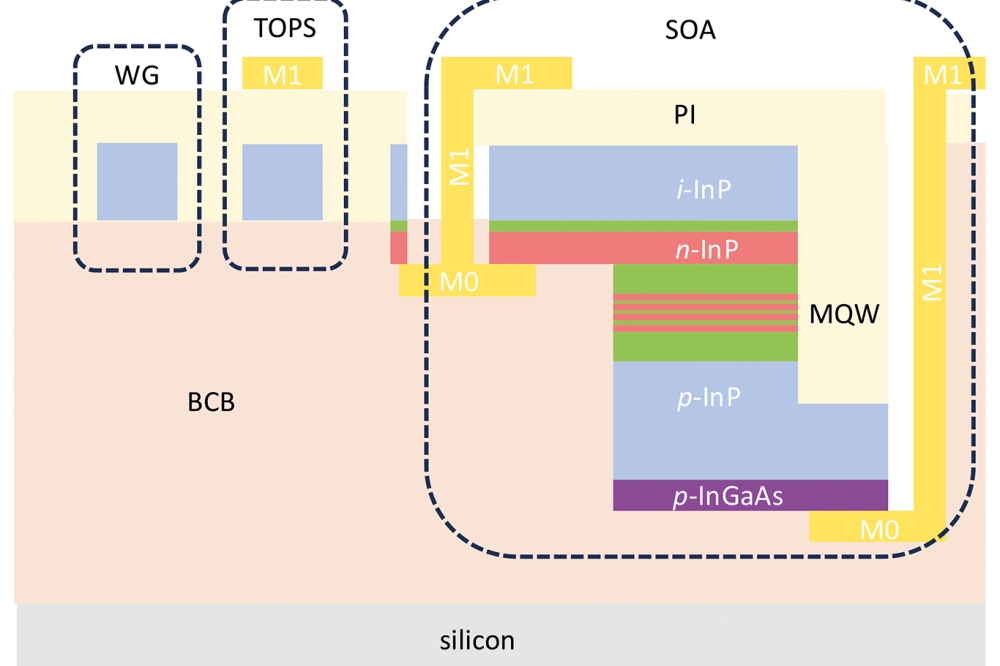
For compact pluggables, a key advantage of InP is associated with the integrated amplification required for a high transmit power. Coherent pluggables incorporating silicon photonics tend to have a low transmit power, typically around just -10 dBm, which is well short of that required by existing optical line systems – they need a transmit power of around 0 dBm. An imperfect solution is to integrate silicon photonics with an erbium-doped fibre amplifier, and add a tuneable optical filter to block out-of-band noise that’s introduced with the additional amplification. But there’s a price to pay, as the introduction of these additional components increases cost and power consumption. A far better option is InP-based pluggables. They include the Infinera ICE-X, which delivers a high transmit power by integrating a semiconductor optical amplifier into the PIC.
What’s next?
In the high-performance embedded segment, evolution vectors include: higher baud rates; improved spectral efficiency and fibre capacity; advanced features related to nonlinear compensation, advanced modulation, forward-error correction, monitoring and automation; support for space-division multiplexing; and novel fibre types, such as multi-core fibres, multi-mode fibres and hollow-core fibres. However, as this sector starts encroaching spectral efficiency limits, there is much discussion over whether it makes sense to have one very high-speed interface (i.e., 3.2 Tbit/s) or multiple lower-speed interfaces (i.e., 2 x 1.6 Gbit /s). InP PICs have a strong role to play in both scenarios, with a proven path to 200+ Gbaud and the ability to integrate transmit and receive for multiple wavelengths into a single PIC. Demonstrating this capability are the latest coherent optical engines produced by Infinera, such as the ICE6 (2 x 800 Gbit/s) and the ICE4 (6 x 200 Gbit/s).
In the pluggable segment, likely introductions include low-power 100 Gbit/s for the metro edge, higher speeds (800 Gbit/s, 1.6 Tbit/s) for metro and data-centre interconnects, and longer reach enabling long-haul use cases. Undergoing debate is the role of coherent technologies inside the data centre, with some vendors targeting campus data centre interconnect applications with simplified 800 Gbit/s coherent engines, such as 800LR. Due to the need to reduce data-centre power consumption – a growing concern as artificial intelligence clusters and workloads are sure to scale – huge strain is being applied to data-centre power and cooling infrastructure. A strong contender to help to relieve this strain are InP modulators. Operating at low voltages and powers, these components are compelling candidates even in non-coherent intensity-modulated direct-detect transceivers that dominate today’s data centres.
Beyond optical communications, InP PICs are a promising technology for a wide range of emerging and potential applications. These include defence, automotive lidar, 3D sensing for wearables and smartphones, solar cells, and medical sensing. This class of PICs could also have a role to play in quantum computing and in neuromorphic computing for AI and machine learning.


