

Integrating microLEDs and MOSFETs
The monolithic integration of microLEDs and vertical MOSFETs offers a promising pathway for making microLED displays.
BY ZHE ZHUANG FROM NANJING UNIVERSITY
Many regard the microLED as the most promising technology for next-generation displays. The primary attributes of this miniature emitter include high brightness, high reliability, a long lifetime and low power consumption. Compared with the organic LED, which is now widely used in smartphone displays and high-end TVs, the inorganic microLED based on III-nitrides is more than ten times brighter and consumes two-to-five times less power. Thanks to these strengths, microLEDs could be deployed in wearable electronic devices operating in very bright environments, such as head-up displays, augmented-reality glasses and cell phones. As some of these consumer products are powered by batteries, the lower power consumption of the microLED is valued, enabling a longer running time between charges. Due to all these advantages, the display industry is now investing in microLED technology, with the hope that it can soon replace OLEDs in many products.
As its name suggests, the microLED is much smaller than its forefather that’s now widely adopted in general lighting. While there is no official definition for the boundary between the two, as a guide, microLEDs are no bigger than 75 µm.
When microLEDs are deployed in displays, their maximum size is governed by the working distance to the screen. The human eye has an angular resolution of 60 pixels per degree. Therefore, the closer the eye is to the display, the smaller the microLEDs must be to maintain the maximum distinguishable resolution. Unfortunately, the efficiency of microLEDs decrease as their size shrinks, an unwanted occurrence that’s referred to as ‘the size effect’. This issue is a major obstacle to the progress of displays based on microLEDs.
As well as microLEDs, switching control transistors are a key component in these displays. Their role is to switch the corresponding microLEDs on and off and control their brightness. By performing these functions, displays can show images and play videos.

Figure 1. Overview of the integration schemes for switching control transistors and microLEDs.
Unfortunately, the microLEDs and transistors that are used in displays tend to be made from different materials and produced using a separate manufacturing process. Blue and green microLEDs are made from GaN-based materials – and red are based on AlGaInP – while transistors are constructed from other classes of semiconductors. Options for the latter include thin-film transistors (TFTs) based on either low-temperature polycrystalline silicon or InGaZnO, or silicon CMOS ICs. The panel housing the TFTs or the CMOS IC is called a backplane, and it has to be integrated with microLEDs to make a display. Establishing an efficient, high-yield process for this integration is another critical challenge facing developers of microLED displays.
The majority of these developers are pursuing an integration technique known as ‘mass transfer’, with a ‘pick and place’ process that transfers millions of microLEDs to the specific positions on the backplane. Today the transfer yield is not high enough for production, and while microLED display prototypes are now in circulation, a significant gap remains towards commercial products.
An alternative approach that avoids this mass transfer process is the monolithic integration of microLEDs and transistors on the same wafer. It is worth noting that the benefits of this form of monolithic integration are not limited to leveraging conventional fabrication techniques, but include the simplification of the process via parallel processing. What’s more, this monolithic approach eradicates the need for high transfer accuracy, and realises an extremely high resolution by conventional photolithography. All these strengths help to trim cost and boost yield, improvements that are highly valued by the display industry.
One team that has adopted the monolithic concept is ours at Nanjing University, China. We are pioneers of the lateral integration of pairs of microLEDs and MOSFETs, both based on the GaN platform. Our trailblazing technology involves the re-growth of a hybrid tunnel junction on a commercial GaN LED epiwafer. The tunnel junction allows us to fabricate microLEDs and MOSFETs with a vertical high-mobility electron channel from the same epiwafer. By drawing on a careful monolithic design, we have demonstrated pairs of microLEDs and normally-off MOSFETs in different sizes. This breakthrough is contributing to the advancing of GaN-based optoelectronic integrated chips, which have the potential to serve in transparent and flexible microLED displays.

Figure 2. (a) Cross-section schematic (left) and transmission electron
microscopy (TEM) image (right) of tunnel-junction LED structure. (b)
Current density-voltage plot of tunnel-junction microLEDs with different
diameters. The inset is the emission image of a 100 µm tunnel-junction
microLED at 1 A cm-2.
Monolithic options
One of the key decisions to make when pursuing monolithic integration is this: heterogeneous or homogeneous? Determining which one is the choice of material for the transistor. If the material for the transistor differs from that used to make the microLED, monolithic integration is heterogeneous; otherwise, it is homogeneous. For heterogeneous integration, fabrication tends to begin by integrating transistor materials on the LED wafer, before fabricating transistors on that wafer.
Initially, we pursued this approach to integration. In 2021, we reported a three-dimensional monolithic microLED display driven by a TFT matrix. For that work, our TFTs were made from the two-dimensional material MoS2. Those TFTs have a mobility of 54 cm2 V-1 s-1, implying that they provide good drive capability for various display applications.
Thanks to the benefits of monolithic integration, we could skip over the precise mass transfer process, and realise a prototypical display with a resolution of 1270 pixels-per-inch. Our success enabled the first concept or demonstration of an inorganic microLED display driven by MoS2 transistors. It is worth noting that the heterogeneous monolithic approach always requires an additional fabrication process to integrate different materials on a single wafer – and threatens to reduce yield and increase cost. In our case, we had to transfer MoS2 materials onto the LED wafer.
More recently, we have advanced to a homogeneous monolithic approach, integrating microLEDs and transistors naturally on a single wafer. Due to the maturity of GaN transistors, both HEMTs and MOSFETs, the key challenge we faced when integrating microLEDs and transistors on a GaN platform was the design of a specific epitaxial structure.
The pairing of a microLED with a HEMT is the earliest and most common proposal for monolithic integration. It’s crucial to position the microLED structure above that for the HEMT because the growth temperature for the microLED is lower than that for the HEMT. The fabrication to integrate the microLED and HEMT usually demands a selective etching process and a metal-based interconnect. To ensure normally-off operation for the HEMT, there’s a need for precise control of the etching process when forming the recessed channel of this transistor.
Another option for stacking a microLED and a HEMT is to use selective-area growth. This involves using a patterned dielectric layer, such as SiO2 or SiN, to define an area for epitaxial growth. As normally-off transistors are always preferred, due to their superiority for energy saving, GaN-based lateral and vertical MOSFETs are compelling alternatives to HEMTs.
Introducing the tunnel junction
Over the last ten years the GaN community has devoted considerable effort to developing a GaN-based tunnel junction, and this is now an established feature within a cascaded LED. The conventional tunnel-junction consists of a heavily magnesium-doped p-type GaN layer and a heavily silicon-doped n-type GaN layer, and operation occurs under reversed bias. This kind of GaN-based tunnel-junction can be grown by MBE or MOCVD. Since the growth atmosphere in an MBE chamber excludes H2 gas, which is used in an MOCVD chamber, the quality and performance of the MBE-grown tunnel-junction outperform that of a similar structure grown by MOCVD.
In 2021, we proposed the utilisation of an MBE-grown tunnel-junction structure on a commercial LED wafer to replace the indium tin oxide current-spreading layer in microLEDs. We inserted an ultra-thin InGaN layer to assist carrier tunnelling in the tunnel-junction (see Figure 2 (a)). The addition of the tunnel-junction reduced the operating voltage of the microLED and enhanced its performance. Through continuous optimisation of the growth conditions, we reduced the forward voltage to around 2.7 V at 10 A cm-2 (see Figure 2 (b)), a value that’s comparable to that of conventional microLEDs.
Essentially, a microLED structure and a tunnel-junction structure are two forms of p-n junction. The difference between them is their operation condition: a microLED operates under a forward bias, while a tunnel-junction works at a reversed bias. Thus, when stacked together, the microLED and tunnel-junction form an n-p-n structure. Fortunately, this n-p-n structure is just right for use in a vertical MOSFET. We were so excited when we recognised this that we immediately designed new hybrid devices, formed from the monolithic integration of microLEDs and vertical MOSFETs.
We discovered that many of the fabrication steps for microLEDs and vertical MOSFETs could be performed in parallel. This applies to the etching process to form microLED mesas and MOSFET trenches, and to the sidewall treatment and passivation process to remove damage and protect both these devices. Drawing on this strength, we carefully designed fabrication procedures that enabled us to successfully make tunnel-junction microLEDs and MOSFETs on a single wafer. We connected each pair of devices with a conductive n-GaN layer (see Figure 3 (a)), which minimises parasitic issues caused by metal interconnects.

Figure 3. (a) Schematics of the monolithically integrated
microLED/MOSFET device. (b) Transfer characteristics of the MOSFET with
different diameters. The inset is the IDS-VGS curve.
Our MOSFETs based on our hybrid tunnel-junction and LED structure are normally-off and exhibit an on/off ratio of around 106 (see inset of Figure 3 (b)). This ratio guarantees fine switching, on and off, of the corresponding tunnel-junction microLED. The typical threshold voltage is around 6 V, high enough to prevent false operation.
An important characteristic of our vertical MOSFETs is that they can scale in size with the microLED. The identical scaling rule ensures that our MOSFETs provide identical driving capability, regardless of the size of the microLEDs, a great asset for deploying our technology in different display applications.
We have examined the performance of our integrated tunnel-junction microLED/MOSFET pairs (see Figure 4). We have found that the current through our microLED can be well controlled by our vertical MOSFET’s gate supply voltage (VG) and anode supply voltage (VDD). Our integrated 60 µm microLED exhibits a high output power of 0.12 mW (around 4.2 W cm-2) at a current of 0.3 mA (around 10 A cm-2) when modulating the MOSFET with a VDD of 5 V and a VG of 16 V. This driving capability in our novel structure is comparable to that of IGZO-based TFTs. That’s sufficient to satisfy the requirements of the driving capabilities for most microLED displays.

Figure 4. (a) Emission images and (b) electroluminescence (EL) spectra
of the integrated MOSFET/microLED at different gate voltages when the
VDD is 5 V. (c) Drain bias modulated current-voltage (I-V)
characteristics and light output power of the integrated device at
different gate voltages.
Adding quantum dots
Ideally, microLED displays should be full colour, because they can then provide high-resolution, vivid images and videos that create a wonderful watching experience for the viewer. To realise a full-colour display, red, green, and blue microLEDs are integrated together on the backplane. If the red, green, and blue microLEDs are fabricated separately on different wafers, issues arise that are associated with the ‘pick and place’ mass transfer process.
To avoid this particular issue, we are pursuing a monolithic solution that utilises quantum dots as colour-conversion materials. We use blue microLEDs to provide blue emission and to also pump quantum dots, leading to green and red emission. Since the red, green, and blue microLEDs should be assembled together as a single pixel, the green and red quantum dots must cover blue microLEDs at specific locations.
This kind of quantum dot transfer is challenging. It demands high accuracy, large-area coverage, low cost and ease of operation. One promising option for high throughout involves developing quantum-dot-dissolved, UV-sensitive photoresists and patterning the photoresist with photolithography. This approach demands a very high solubility for the quantum dots in the photoresists. Unfortunately, products that combine quantum dots and conventional photoresists are yet to be widely available.
Due to this state of affairs, we have developed an advanced fabrication technique for patterning quantum dots on blue microLEDs that involves photolithography and dry etching. We have turned to double layers of resists, including a negative photoresist and spin-on-glass, to enhance the stability of the quantum-dot patterns during the fabrication process. With this approach we have fabricated green and red quantum dot patterns as small as 2 µm in size on a 4-inch wafer (see Figure 5 (a)). Note that the 2 µm size is the limitation of our contact aligner, but not our technique. We believe that the size of quantum-dot patterns can be continuously scaled down with advanced steppers.

Figure 5. (a) The green and red quantum dots pattern on a 4-inch wafer
with sizes of 2 µm. (b) Display demonstration of a microLED array with
green/red quantum dots. The insert is a magnified fluorescence
microscope image.
By simply repeating the patterning process for green and red quantum dots, we have demonstrated a red-green-blue microLED array with each chip size less than 10 µm (see Figure 5 (b)). Through monolithic integration with GaN-based MOSFETs, as discussed above, we can go on to realise full-colour microLED displays with a GaN platform. Since our entire fabrication procedures are compatible with standard processes, our techniques are ready for transfer to mass production.
Our progress is an important contribution to the monolithic integration of GaN-based microLEDs with transistors. Such exciting results have established a new route towards achieving full-colour displays based on a GaN platform, which may go beyond the heterogeneous integration limit and spearhead the future for microLED displays.
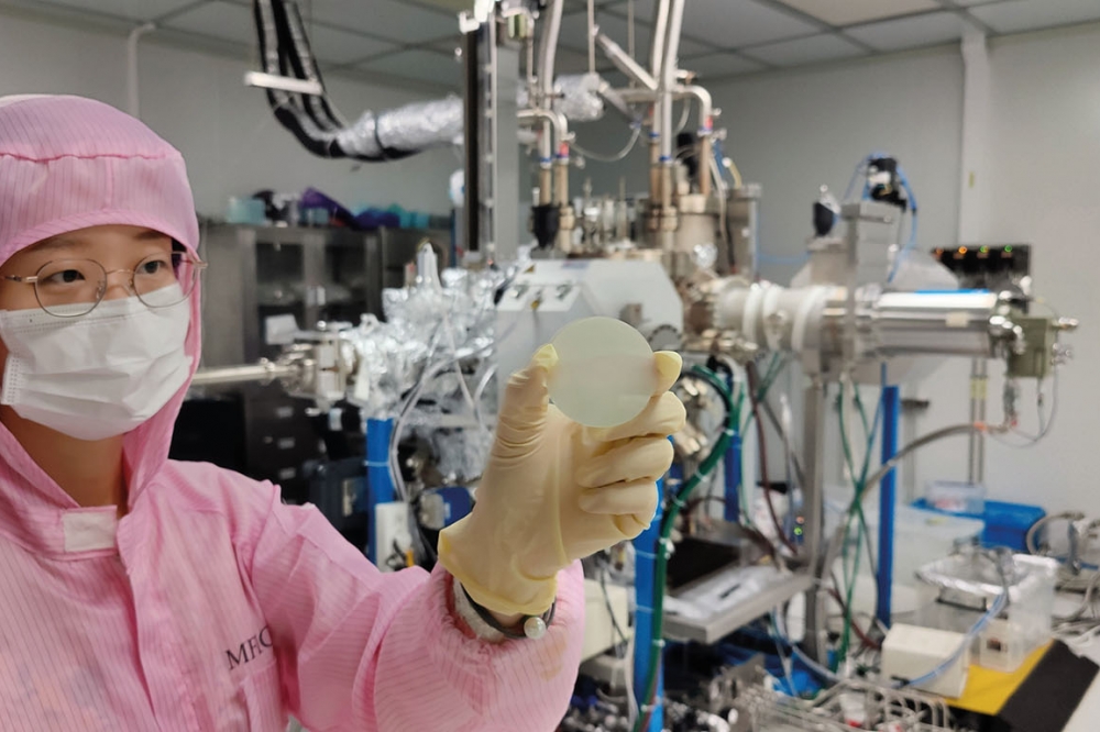
Main image: Yimeng Sang holding a 2-inch green LED wafer with a tunnel junction, regrown by MBE behind her.
Further reading
Y. Sang et al. IEEE Electron Device Letters 44 1156 (2023)
F. Xu et al. IEEE Electron Device Letters 44 1320(2023)
W. Meng et al. Nature Nanotechnology 16 1231 (2021)
Y. Wu et al. Photonics Research 9 1683 (2021)


