Loading...
News Article

Tunnelling junction enhances deep UV LEDs
News

Chinese team achieve lowest operating voltage for deep UV LEDs and enable disinfection and water/air purification

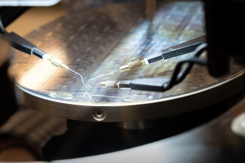
Researchers from Wuhan University and Ningbo ANN Semiconductor in China have made significant progress in improving optoelectronic performance for deep ultraviolet (UV) LEDs.

“We propose the implementation of an ultrathin tunnelling junction (UTJ) technology platform in deep-UV LEDs as a solution to the challenges of high series resistance and deep-UV light absorption. In our study, we successfully develop 275 nm high-power UTJ deep-UV LEDs, achieving the lowest voltage of 5.7 V to date, which is enabled by minimizing electrical losses for hole injection.” said Shengjun Zhou, a professor at Wuhan University who directed the research.

The intriguing properties of deep UV light and its potential applications make it an attracting subject for fundamental studies. The wavelength range of deep-UV (200-280 nm) has been found to be highly effective in sterilisation and disinfection by damaging the DNA and RNA of bacteria and viruses. However, the low light output power and high operating voltage of deep-UV LEDs make it difficult for current LEDs integrated deep-UV light sources to meet the sterilisation performance targets of effective irradiation distance and exposure time.

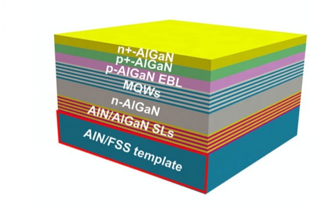
To address these issues, the researchers from Wuhan University proposed to introduce the UTJ as a direct contact layer in deep-UV LEDs for minimising the electrical losses. The schematic illustration above shows the deep-UV LED epitaxial structure grown on AlN/Flat Sapphire Substrate template

They observed the formation of Mg-Si co-doped n-AlGaN during the high-temperature growth of UTJ and discovered that the UTJ can form Ohmic contact with the high-work-function Ni/Au electrode. Furthermore, the encapsulation of UTJ deep-UV LED with Zener diode, fluorine resin, and optimally designed glass lens was demonstrated to improve the reliability and optical performance.

They developed a high-efficiency sterilisation deep-UV light source integrated with 120 UTJ deep-UV LED chips and conducted the experiments on the killing effect of deep-UV light source on multiple pathogenic microorganisms and flowing water sterilisation.

Zhou and colleagues say that the findings are significant and have the potential to enhance the utilisation of deep-UV light sources for water/air purification and disinfection.

Reference

'High-Power AlGaN-Based Ultrathin Tunneling Junction Deep Ultraviolet Light-Emitting Diodes' by Shengjun Zhou et al; Laser & Photonics Reviews, 2023

SPONSOR MESSAGE

Secure Your Hydrogen Supply

A study supply of high-purity hydrogen is critical to semiconductor fabrication. Supply chain interruptions are challenging manufacturers, leading to production slowdowns and stoppages. On-site hydrogen generation offers a scalable alternative for new and existing fabs, freeing the operator from dependence on delivered gas.

Plant managers understand the critical role that hydrogen plays in semiconductor fabrication. That important job includes crystal growth, carrier gas, wafer annealing, and in the emerging Extreme UV Lithography (EUV) that will enable new generations of devices. As the vast need for semiconductors grows across all sectors of world economies, so does the need for high-purity hydrogen.

Take control with Nel on-site hydrogen generation.

Read more
QD company Quantum Science expands into new facility
Innoscience files lawsuit against Infineon
Riber revenues up 5% to €41.2m
Forvia Hella to use CoolSiC for next generation charging
Photon Design to exhibit QD simulation tool
Ortel transfers CW laser fabrication to Canada
Luminus adds red and blue multi-mode Lasers
PseudolithIC raises $6M for heterogeneous chiplet tech
Mesa sidewall design improves HV DUV LEDs
IQE revenue to exceed expectations
'Game-changing' VCSEL system targets clinical imaging
German start-up secures finance for SiC processing tech
Macom signs preliminaries for CHIPS Act funding
IQE and Quintessent partner on QD lasers for AI
EU funds perovskite tandems for fuel-free space propulsion
EU to invest €3m in GeSi quantum project
Transforming the current density of AlN Schottky barrier diodes
Turbocharging the GaN MOSFET with a HfO₂ gate
Wolfspeed launches Gen 4 SiC MOSFET technology
Report predicts high growth for UK's North East
Element Six unveils Cu-diamond composite
SemiQ launches hi-rel 1700V SiC MOSFETs
Lynred to exhibit Eyesential SWIR sensor for machine vision
Thorlabs buys VCSEL firm Praevium Research
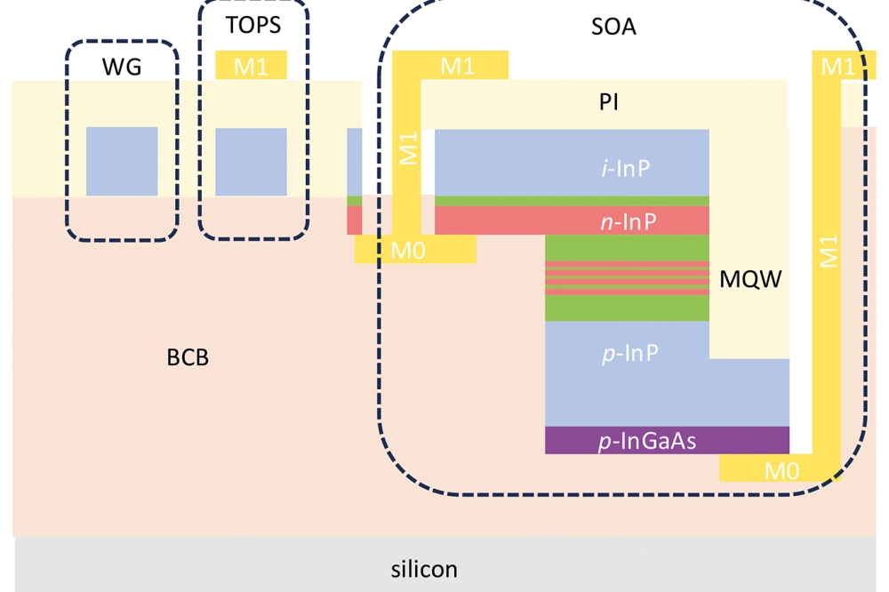
Advancing tuneable InP lasers on a heterogeneous platform
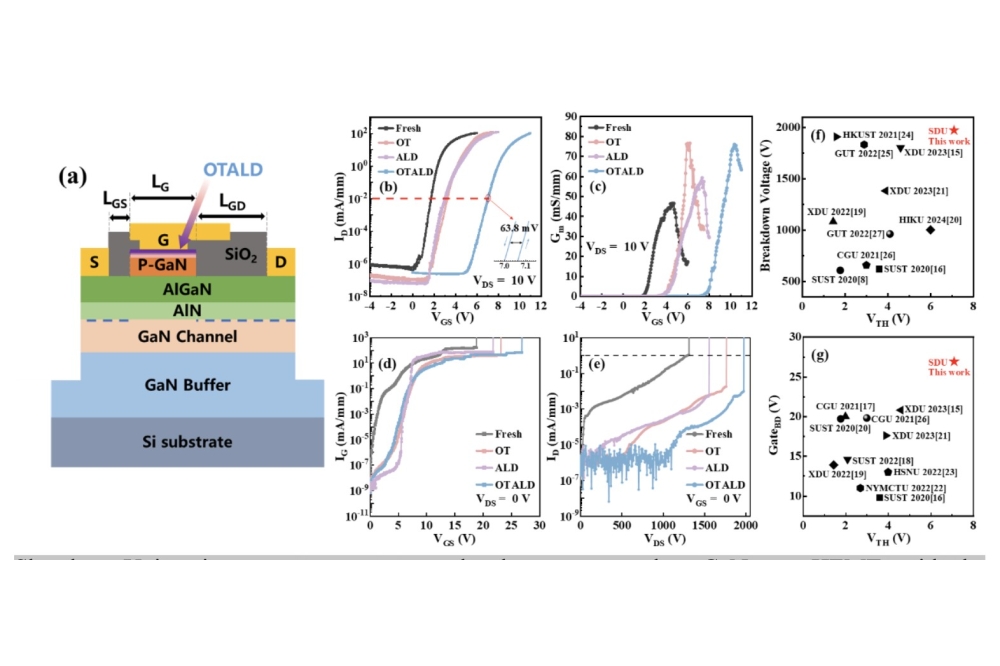
P-GaN gate HEMTs have record threshold voltage
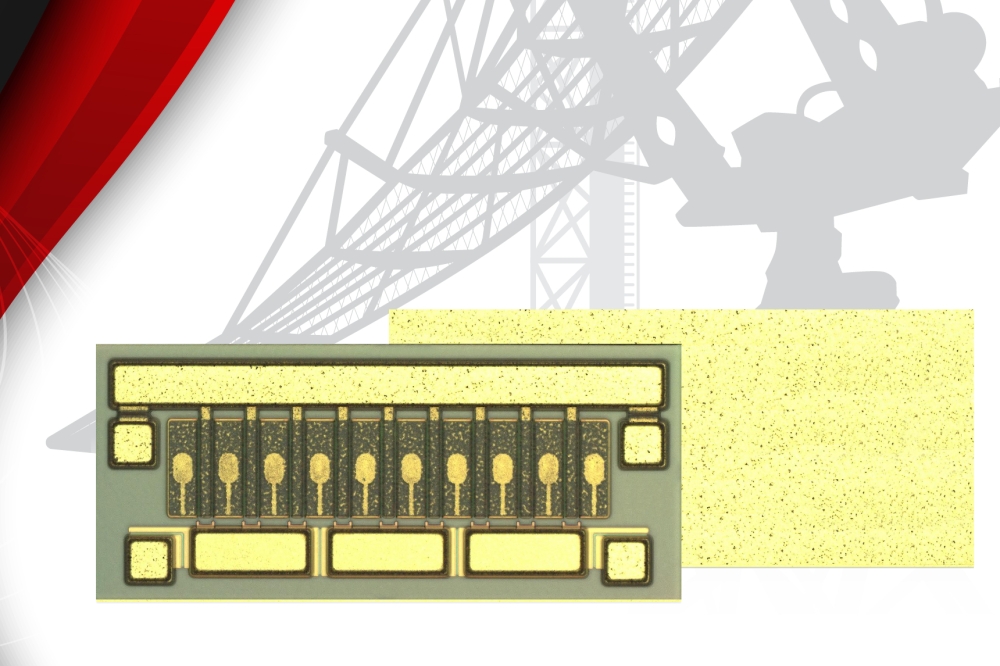
Guerrilla RF releases GaN power amplifier dice
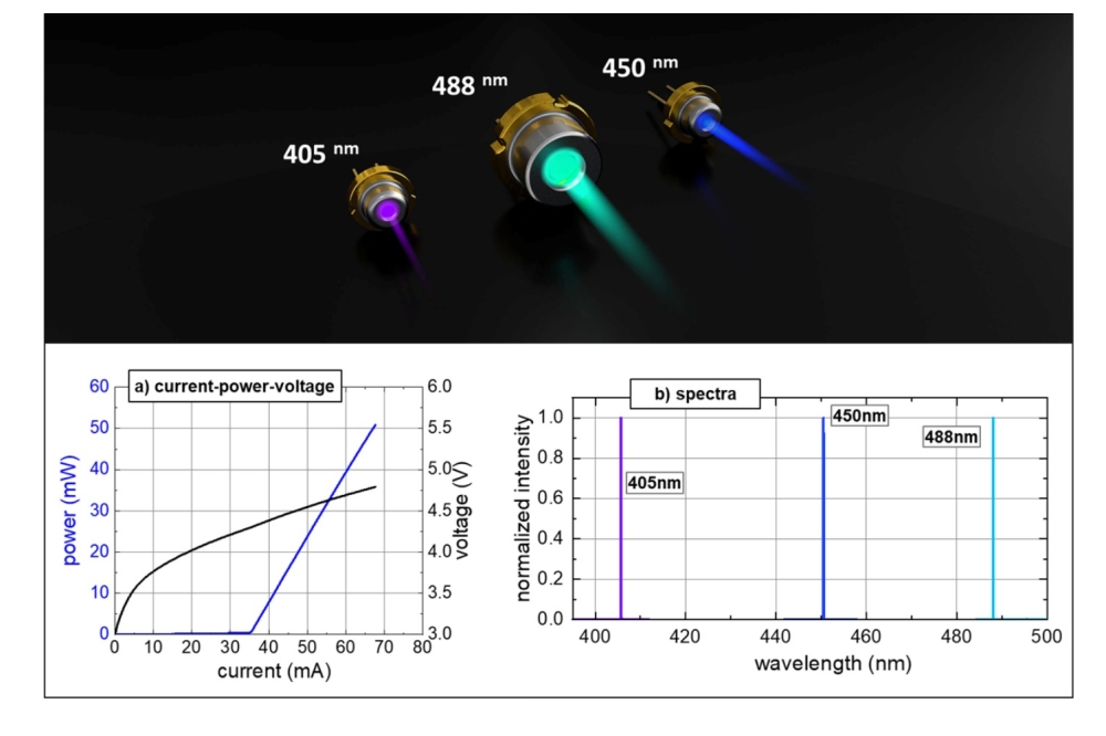
Narrow-linewidth DFB lasers now at 405 and 488nm
Researchers develop tech for future fast-charging stations
Vermont GaN Tech Hub awarded nearly $24M
Onsemi completes buy-out of Qorvo SiC JFET business
Quantum Science announces Innovate UK funding
×
Search the news archive

To close this popup you can press escape or click the close icon.
Logo
x
Logo
×
Register - Step 1

You may choose to subscribe to the Compound Semiconductor Magazine, the Compound Semiconductor Newsletter, or both. You may also request additional information if required, before submitting your application.


Please subscribe me to:


You chose the industry type of "Other"

Please enter the industry that you work in:
 
x
Adblocker Detected
Please consider unblocking adverts on this website