
Empowering electric vehicles with superior SiC
SmartSiC substrates hold the key to ramping volumes of better SiC devices for automotive and industrial applications.
BY EMMANUEL SABONNADIÈRE, CHRISTOPHE MALEVILLE AND CYRIL MENON FROM SOITEC
In September 2021, SmartSiC made its debut in Compound Semiconductor magazine. Pioneered by our company, Soitec, this novel material technology is a game-changer within the SiC industry: it is enabling a new generation of engineered substrates that consist of a thin layer of single-crystal SiC, bonded on a polycrystalline SiC wafer. Now two years on from this unveiling, SmartSiC is starting to fulfil its potential, delivering impressive results.
The impact of SmartSiC will be colossal. It has fundamentally changed perspectives for SiC, especially for 200 mm acceleration, and it is starting to reshape the SiC industry with a much greener technology. The great strengths of SmartSiC, compared with incumbent single-crystal SiC wafer, include an unparalleled ten-times hike in re-use capability and an eight-fold enhancement in electrical conductivity. Due to these massive improvements in key metrics, SmartSiC is opening new frontiers for high-performance SiC devices and their applications.
As well as these exceptional capabilities at the wafer level, SmartSiC is demonstrating its capability to produce a foundation that ensures better diodes and transistors. Measurements reveal a reduction in the drain-source on-resistance of 1200 V MOSFETs of between 10 percent and 15 percent, and around a 15 percent decrease in forward-voltage at a rated current in 650 V SiC diodes. These noteworthy improvements in device-level performance translate into a significant advantage in the fabs, with the opportunity for around a 25 percent increase in the number of high-quality die that can be produced from every 200 mm wafer for 25 mm² dies.

Leading the way, STMicroelectronics is the initial adopter of SmartSiC technology. Its collaboration with us has been dedicated to the rigorous automotive qualification of SmartSiC. The ultimate goal for our partnership is to qualify SmartSiC on ST SiC MOSFET technology in mid-2024, with products based on SmartSiC available from Q3 2024 onwards. Meeting this target will position both of us at the forefront of innovation in the EV sector.
Our SmartSiC technology continues to evolve and improve. Recently, we increased the crystal quality of our SmartSiC wafers with a specific epitaxy preparation, realised before the layer transfer of single-crystal SiC. Thanks to this advance, we have drastically reduced the basal plane dislocation density in our material. In turn, this will lead to better device performance.
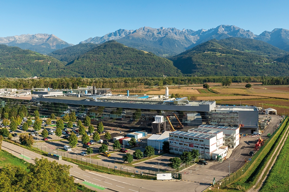
This year, SmartSiC became a ‘must-have’ technology for key leaders in the SiC industry. With over a thousand prototypes under assessment and more than thirty prospects and clients, SmartSiC is now being adopted. High-volume production will take place at our new plant, Bernin4, which opened this September, following the installation of initial industrialisation lines over the summer months. When fully up and running, this fab will have a capacity of 500,000 wafers per year. Note that the production process used in this fab is flexible, starting with 150 mm wafers and adding 200 mm wafers in the first half of 2024. Once the ten-fold re-use goal is attained, another significant advantage will emerge: a secured production process, thanks to reserves of refreshed wafers that we will hold.
To put it succinctly, given all the strengths of SmartSiC, this technology is an obvious choice for any SiC device maker wanting to process 200 mm wafers – and that’s before considering current global scarcity of this material.
High-volume manufacturing
The unparalleled performance of SmartSiC is not just attracting the attention of makers of SiC power devices. Our technology is also garnering significant attention further along the supply chain, from Tier 1 and OEM companies within the automotive industry. What pleases them is that it will not be long before we attain IATF and ISO9001 certification at Bernin4, aligning with the standards of our other manufacturing plants in Bernin and Pasir-Ris. Note that our company, and our SmartSiC portfolio, are deeply committed to an impressive environmental, social and governance agenda.
High on our agenda when developing our production process is energy efficiency, with much effort directed at reducing energy consumption. Perfectly aligning with this objective, SmartSiC is starting to play a pivotal role in realising substantial reductions in carbon footprint when compared with traditional bulk SiC materials. Such a synergy is vital in supporting the ongoing EV revolution, which is making a crucial contribution to combating climate change. Our company, and SmartSiC, are actively aiding this cause at various levels, from wafer production to power device development and system integration.
Building Bernin4 has not been easy. As well as a supply crisis in construction materials, there’s been a flurry of industrial construction projects in the Grenoble region. Yet despite these issues, we have completed the 2000 m2 clean room for SmartSiC on time, with just 18 months elapsing from breaking ground to the construction of the first prototypes.

Our state-of-the-art clean room is seamlessly integrated into our pre-existing infrastructure. Due to this, we have established crucial links with Bernin 2 (300 mm silicon-on-insulator wafers), raw materials storage and the finished products warehouse. This strategic connectivity enhances operational efficiency by ensuring optimised flow and maximising flexibility for the facility.
To provide a high-skilled workforce for Bernin 4, we are gradually transferring over operators, technicians and engineers trained on the SmartSiC pilot line at CEA/LETI in Grenoble. These staff are being integrated into the Bernin 4 organisation to manufacture the first industrial prototypes. Bernin 4 benefits from the same digital resources supporting the other plants on the site: a semiconductor manufacturing execution system, a process control system, and manufacturing equipment that’s monitored using statistical process control, fault detection and classification, and computerised maintenance management systems. The production line is scheduled to receive ISO 9001 certification by October 2023, and plans are in place to obtain IATF certification in 2024.
A quick, efficient ramp up
One of the great strengths of our SmartSiC industrial line is that we are able to manufacture more than 10 SmartSiC substrates from a single-crystal SiC substrate.
By adjusting the single-crystal SiC supply volumes, we can deliver a very steep ramp up in the production of SmartSiC substrates. This is accomplished by injecting a larger quantity of single-crystal SiC from the start of production, to load the line, a point illustrated in Figure 1. Starting with just over 11,000 SiC wafers, we can yield around 10,000 during the first cycle (Figure 1 shows the number of single-crystal SiC wafers present in the line as a function of the cycle time, with the colour indicating the origin of the wafers – in blue, 1st injection; in red, 2nd injection; in orange, 3rd injection; and so on).
During our industrialisation of SmartSiC, we control ramp up, and then we retain a steady state by adjusting the level of injection of single-crystal SiC substrates in the line. By using single-crystal SiC substrates over N cycle times – an approach that provides a degree of inertia – we ensure a level of resilience, in terms of the number of SmartSiC wafers that we produce, by catering for the possibility of irregularity in the number of single-crystal SiC wafers injected in each cycle time.
As well as pioneering SmartSiC, we are playing a key role in driving the development of the polycrystalline SiC supply ecosystem. This effort includes a joint-development agreement with Mersen, a renowned French-based company with broad materials expertise. Together we are crafting the most efficient polycrystalline SiC wafers. Our joint strategy is to qualify suppliers across different regions. We have already established long-term contracts with two suppliers and we are actively engaging with a third. Notably, Bernin 4 can accommodate a high degree of flexibility from our suppliers, as this facility allows for a seamless transition between 150 mm and 200 mm wafers.

Targeting a 10,000 SmartSiC production per cycle time with a steep ramp up (permanent regime since the 2nd cycle time), around 11,000 single-crystal SiC substrates are injected for the first cycle time to initially load the line. To compensate for losses linked to yield, for of each following cycles, roughly 600 single-crystal SiC substrates are added per cycle time. Considering a maximum number of refresh of 15x, the first injection of SmartSiC has to be replaced at the 16th cycle time, equating to around 5,000 single-crystal SiC substrates in this example. Losses linked to yield are compensated for in each of the following cycles (roughly 800 single-crystal SiC substrates per cycle time). The graphs show the number of monoSiC substrates injected in the line every cycle time (left) and the number of SmartSiC wafers produced versus cycle time (right). Based on a realistic industrial scenario, we can see that the manufacturing kinetics are such that the number of SmartSiC wafers generated exceeds rapidly the number of single-crystal SiC substrates inserted to reach a factor of 10x across N cycle time
Automotive and industrial markets
Our SmartSiC is targeting markets that are tipped for phenomenal growth. For the Light Vehicles market, worldwide production is forecast to increase at a low-to-mid single digit compound annual growth rate (CAGR) through to 2030. Within this, battery EVs are the dominant driving force, predicted to climb at a CAGR of above 20 percent. Thanks to this rapid growth, the CAGR for SiC modules is 32 percent. In addition, there is a profound shift towards electrification in industrial applications, providing additional opportunities for SmartSiC.
We will quickly penetrate these markets by ramping our production by a factor of ten in just 18 months at our Bernin facility. Our expectation is that by 2030, the SmartSiC share of the SiC market will be higher than 30 percent. The SmartSiC wafer manufacturing process also reduces CO2 emissions by 70 percent compared with current monocrystalline SiC substrates.
Our progress aligns with one of our key values, which is contributing to a reduction in climate change. We are deeply committed to environmental, social and governance performance, with considerable effort directed at reducing water and energy consumption, as well as minimising waste. Moreover, our strategic SiC programme that led to the development of SmartSiC involved a strong commitment to greener values, while delivering superior results compared with bulk SiC.


