
III-Nitride field-emission vacuum transistors
Field-emission transistors featuring III-Nitrides unlock the door to
robust, compact vacuum-electronics-based circuits that deliver high
powers at high frequencies.
BY PAO-CHUAN SHIH AND TOMÁS PALACIOS FROM MIT
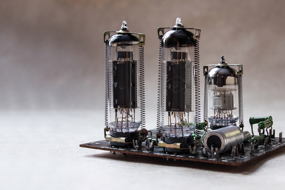
Vacuum based electronics have an incredibly rich and successful history. At the beginning of the twentieth century they enabled the first electric switch, based on a vacuum triode. Vacuum tubes also lay at the heart of the first programmable general-purpose electronic computer, known as ENIAC, which was built in the 1940s. Its construction revolutionised calculation speed, being about a thousand times faster than the electro-mechanical machines of the day. However, this trailblazing computer had a substantial footprint and lacked green credentials, being 2 m by 1 m by 30 m in size, occupying 170 m2, and consuming 150 kW of electricity.
Since the invention of solid-state transistors in 1947, semiconductor devices have gradually replaced vacuum electronics, due to lower production costs and ease of scaling. Due to this, vacuum electronics are now only used in few niche applications. Where they are still having an impact is in travelling wave tubes and klystrons, which produce intense high-frequency signals at 10-100 GHz and above 100 GHz, respectively, thanks to scattering-free electron transportation and a high breakdown field in the channel (see Figure 1). Additional merits of vacuum electronics are robustness at high temperatures and a capability to withstand radiation environments that degrade solid-state devices.

Figure 1. Electron transport in (a) semiconductor and (b) vacuum
channels. Scattering-free transportation and a high breakdown field in
vacuum make vacuum channels excellent candidates for high-power and
high-frequency electronics. Theoretically, degenerately n-doped
III-Nitrides, such as AlGaN alloys, can have a low electron emission
barrier thanks to their low electron affinities, making them excellent
vacuum emitters.
Key to leveraging the excellent potential of the vacuum channel is the injection of electrons into vacuum. A conventional approach for realising one form of electron emission, known as thermionic emission, is to heat the cathodes so that they give the electrons enough energy to overcome the work function barrier between the solid and vacuum. However, this requires high temperatures, hampering the construction of compact devices. Additional factors limiting the deployment of thermionic cathodes in large-scale circuits and systems are high power consumption, a need for cooling, and a relatively low switch speed.
Finding favour with field emission
Fortunately, all these issues can be addressed by turning to field emission. With this approach, electric fields control the tunnelling distance for the emission of electrons into vacuum. A number of semiconductors and metals have already been investigated as field emitters, but issues have often arisen, such as a limited gate control efficiency, less-than-ideal current densities, and device instability.
One class of material that promises to avoid these pitfalls is the III-Nitrides, such as GaN, AlGaN, and AlN. Recently, these compounds have been attracting attention due to their engineerable electron affinities (see Figure 1). Electron affinities reduce when the aluminium composition of the AlGaN alloy increases, and when the surface polarisation is changed from metal polar to N polar. According to theory, degenerately n-doped semiconductors with low electron affinities should have very low work functions, leading to a high emission current density and a low operating voltage.
Despite the great potential that III-Nitrides have for field-emission applications, research efforts have focused on ‘bottom-up’ approaches, growing these materials as nanostructures. Reports are often limited to two-terminal geometries with operating voltages usually larger than a few hundred volts. The lack of a third control terminal is a significant drawback, limiting their use in applications such as power amplifiers, high-voltage switches, and computation circuits for harsh environments.

Figure 2. There are three key building blocks for compact
field-emission-based vacuum transistors: a self-aligned gate, which
enables transistor-like behaviour and a low operating voltage for
electron emission; sharp, uniform emission tips that are critical for
uniform electron emission for reduced operating voltage and high current
density; and an integrated anode with an in-situ vacuum cavity package,
which is necessary for circuit-level scale-up capability.
Over the last five years, our team at MIT has been developing and improving III-Nitride field-emission-based vacuum transistors. Our efforts have involved identifying three key challenges and developing new technologies to address them: (1), a compact self-aligned gate; (2), sharp and uniform field-emitter tips; and (3), an integrated anode (see Figure 2).
To tackle the lack of gate terminals, which has traditionally limited the applications of III-Nitride field emission devices, we have developed self-aligned gate structures for this class of material. For this development, we have drawn on work by other groups that developed silicon and metal field-emitter tips. Our team adopted a ‘top down’ approach, using dry etching to produce well-organised GaN field-emitter arrays. We deposited and defined a self-aligned gate structure on these field-emitter arrays, enabling them to deliver excellent gate-control capability and a transistor-like behaviour at operating gate voltages below 100 V.
In addition to introducing a self-aligned gate, improvements to the uniformity and sharpness of field emitter tips are essential for increasing the performance of field-emission-based vacuum transistors. To ensure field emission, there’s a need for high electric fields, which reduce the electron tunnelling barrier from the Fermi level to the vacuum level. This quantum tunnelling mechanism has an exponential dependence on the electric fields on the surface – the stronger the field, the higher the electron emission. It is also possible to locally enhance the electric field by altering the shape of emitter tips. Due to this, uniform and sharp tips are critical to realising uniform electron emission in field-emitter arrays, and thus ensuring an increased current density.

Figure 3. The process flow of the GaN field-emission-based vacuum
transistors and the cross-section device diagrams after key steps. The
anode electrode is not yet integrated in these devices.
Our third initiative – following development of the gate structure and the GaN emitter tips – has involved the integration of the anode electrode in our state-of-the-art field emitters. By taking this step, we have been able to form three-terminal fully-integrated vacuum transistors, which are necessary for scale-up applications, such as vacuum-electronic-based integrated circuits.
Efforts on this front have enabled us to reliably produce an integrated anode with a sub-1 µm channel length. Note that we are able to alter the channel length by adjusting multiple parameters during device fabrication. Our approach also provides us with the potential to seal the vacuum cavity, which relaxes restrictions on vacuum packaging and circuit-level integration. We will soon publish the details of our anode-integration technology and describe its impact on device performance.
Engineering the emitter
Etching and cleaning steps have been used to fabricate our III-Nitride field-emitter transistors (see Figure 3 for an overview of the main steps). We begin with GaN-on-silicon coupons, which are cut from a 6-inch wafer. Using plasma dry etching with nickel hard mask that’s defined by an e-beam lithography and lift-off process, we form GaN field emitter arrays on these coupons. The tips of the GaN emitters are sharpened by wet-based digital etching (see Figure 4, as well as Step 1 in Figure 3).
During one cycle of digital etching, the sample is initially treated with a mixture of H2SO4 and H2O2 to oxidise the GaN surface (step 1). After this, deionised water removes the residual chemicals (step 2), before the surface oxide layer is etched away with dilute HCl (step 3), and the sample rinsed once more by deionised water (step 4). Following a few cycles of digital etching, it’s imperative to renew the chemicals, because H2O2 decomposes and the temperature of the mixture of H2SO4 and H2O2 decrease over time. We have found that three cycles of this wet-based digital etch sharpen Ga-polar GaN pyramid tips by 5 nm, enabling reliable fabrication of uniform GaN emitter tips with a sub-20-nm tip width in field-emitter arrays.
After forming GaN field-emitter arrays with sub-20-nm emitter tips, we deposit SiO2 and Al2O3 by PECVD and ALD, respectively (step 2 in Figure 3). Adding a SiO2 layer improves device stability under the gate pad region, while coating with Al2O3 protects the sharpened GaN emitter tips from subsequent fabrication steps, key to ensuring a high fabrication yield and good device performance.

Figure 4. (a) A simplified device diagram representing measurement setup
and (b) a cross-sectional scanning electron microscopy (SEM) image of
the fabricated GaN emitter tip with a self-aligned gate. (c)
Transmission electron microscopy (TEM) image of the GaN tip confirms the
tip width of 10-12 nm. SEM images of the GaN emitter tip (d) before and
(e) (f) after the digital etching (DE) confirm the effective tip
sharpening of this DE technology. One cycle of DE consists of H2SO4+
H2O2 for oxidisation and dilute HCl for oxide removal. This process
enables the fabrication of sharp and uniform tips in field emission
arrays. (b) Cross-sectional SEM and (c) TEM images provided by Prof. Bruce Gnade’s group at Southern Methodist University.
These subsequent fabrication steps begin with the addition of a SiO2 layer by PECVD, using a tetraethyl orthosilicate (TEOS) precursor. The growth of a conformal chromium layer by sputtering follows (step 3 in Figure 3). It is the SiO2 and chromium layers that form the gate stack of the GaN field-emission vacuum transistors.
Finally, we deposit a thick SiO2 layer with the TEOS precursor by PECVD. We then planarize the device surface through carefully timed dry etching on this TEOS SiO2 layer (step 4 in Figure 3). We then dry etch the chromium gate metal on top of the emitter tips, with the TEOS SiO2 layer acting as a hard mask (step 5 in Figure 3). After forming metal contacts on both GaN and the gate metal, chromium, GaN emitter tips are exposed by a carefully timed dry etch. A short wet etch using a buffered oxide etchant then removes the remaining SiO2 layer and the protective Al2O3 layer (step 7 in Figure 3). Using this process, we have reproducibly fabricated three different generations of GaN field-emitter arrays with self-aligned gates and sub-20-nm tip widths.

Figure 5. (a) (b) Scanning electron microscopy images and (c) transfer
characteristics of the state-of-the-art GaN field emitter array with a
self-aligned gate. The device has good gate control of the emission
current (IE) and anode current (IA) with an above 105 on-off ratio and
low gate leakage (IG), which is less than 10 percent of IA at on state
(VGE = 50 V). The fitting (purple dashed line) of the anode current
confirms that the current conduction is dominated by field emission.
Promising potential
We have characterised our field emitter arrays in an ultra-high vacuum chamber with a base pressure below 2 x 10⁻⁹ Torr. When determining transfer characteristics, we applied a gate-emitter bias voltage (VGE) to extract electrons out from the emitter tips, and used a high voltage on the suspended anode terminal – between 500 V and 1000 V – to collect the emitted electrons (as shown in Figure 4 (a)). While we could adjust the anode-emitter distance by moving the sample stage up and down, for all our measurements we fixed this distance to 1-2 mm.
Our latest generation of GaN field-emitter arrays feature self-aligned gates with uniform sharp tips in the array, surrounded by sacrificial blunt tips that help manage the peak electric field in dielectric layers, leading to improved device stability (see Figure 5 (a) and (b)). Our best field-emitter arrays have a good on-off ratio in anode current, a low gate leakage (it is less than 10 percent of the anode current in the on state), and a current density of 10 A cm-2 at a gate-emitter voltage of 50 V – to our knowledge, that’s the highest current density among all the field-emitter arrays reported in the literature (see Figure 6 (a)). Note that the relatively high noise levels in the emitter and anode currents are a measurement artefact related to the high-voltage source measure units. The current-voltage curves can be well fitted by field emission equations, such as the Murphy-Good model.
Thanks to the combination of a compact self-aligned gate structure and uniform and sharp GaN emitter tips, our field-emitter arrays are state-of-the-art for III-Nitride field emission devices, and deliver the highest field-emitted current density in the literature at a gate-emitter voltage of 50 V (see Figure 6 (a)). For these structures, the current density is based on the total device area for the field-emitter array with its self-aligned gate.

Figure 6. Benchmarking plots of (a) current density (JA) versus turn-on
voltage (VGE,ON) and (b) maximum anode current per tip versus
gate-emitter voltage (VGE) for maximum anode current reported. These
devices have the highest current density (10 A/cm2) and comparable
current per tip (35 nA /tip) at VGE = 50 V. The maximum current per tip
of reported silicon field emission arrays at VGE = 50 V is about 100 –
500 nA/tip.
In addition to the current density, a key metric for these field-emitter arrays is the emission current per tip. Ideally arrays have a high average emission current per tip under low bias conditions, because this enables these devices to deliver a high level of efficiency when serving in integrated circuits and power applications. Our best GaN field-emitter arrays have a maximum average-emission-current-per-tip of 35 nA, while those based on HfC-coated silicon field-emitter tips have demonstrated 100-500 nA per tip, also for a gate-emitter voltage of 50 V. Based on these results, it is clear that there is still room for improvement in the current density in III-Nitride devices.
We have identified significant opportunities for making additional gains in device performance. These pathways include: reducing the gate-emitter distance, now about 150 nm, to enable an increase in gate control over electron emission from the emitter tips (see Figure 7 (a)); sharpening the tip width to below 10 nm, to enhance the local electric field (see Figure 7 (b)); and leveraging low-electron-affinity III-Nitride semiconductors or low-work-function materials (see Figure 7 (c)).
Initial efforts on these fronts have included the fabrication of silicon field-emitter arrays with a gate-emitter distance below 50 nm and a sub-5-nm tip radius in prior work. Encouragingly, the turn-on voltage – that is, the gate-emitter voltage to turn the device on – is around just 10 V. However, these devices suffer from performance variations, associated with tip-size variability and the narrow device geometry.

Figure 7. (a) Proposed fully-integrated field-emission-based vacuum
transistors with advanced modifications for performance improvement, and
the estimated emission current per tip with a (b) scaled emitter tip
radius and (c) reduced work function in the emitter tip. The dashed
lines in (c) indicate the region where the assumption of estimation is
invalid dueto high electric fields corresponding to the emitter work
function. The gated emitter is assumed to have a (300 nm)2 device area
and the breakdown voltage in the vacuum channel is assumed to be more
than 200 V to estimate the possible output power density.
We hope that by leveraging the low-electron-affinity of III-Nitride materials and the polarisation engineering of the surface dipole, we will be able to produce field emitters with an even lower work function and a reduced energy barrier for electron emission (see Figure 7 (c)). Nevertheless, our preliminary experiments on both n+ aluminium-rich AlGaN and n+ N-polar GaN are yet to offer a clear improvement in device performance. To address this particular shortcoming, we plan to undertake a material-dependent optimisation of the etching processes for emitter tip formation.
While there is still more work to do, we have a strong foundation to build on. Our GaN field-emitter arrays with a self-aligned gate and uniform, sharp emitter tips have enabled us to demonstrate state-of-the-art field-emission-based vacuum transistors with the highest current density at a gate-emitter voltage of 50 V. Once we have made further improvements in performance by integrating anode structures and applying advanced materials engineering we are confident that our III-Nitride field-emission-based vacuum transistors will be able to play an important role in tomorrow’s high-frequency, high-power, and harsh-environment electronics.
FURTHER READING / REFERENCE
• Pao-Chuan Shih et al. “Self-Align-Gated GaN Field Emitter Arrays Sharpened by A Digital Etching Process,” IEEE Electron Dev. Lett. 43 422 (2021)
• Pao-Chuan Shih et al. “Wet-based digital etching on GaN and AlGaN,” Appl. Phys. Lett. 120 022101 (2022)
• Pao-Chuan Shih et al.. “GaN Field Emitter Arrays with JA of 10 A/cm2 at VGE = 50 V for Power Applications,” 68th International Electron Devices Meeting (IEDM), December 2022
• Pao-Chuan Shih, “Vacuum Transistors Based on III-Nitrides Field Emitter Arrays with Self-Aligned Gate,” PhD Dissertation, Massachusetts Institute of Technology, 2023.


