Loading...
News Article

Diamond Foundry shrinks EV inverters

News

Power electronics unit is six times smaller than that of a Tesla 3

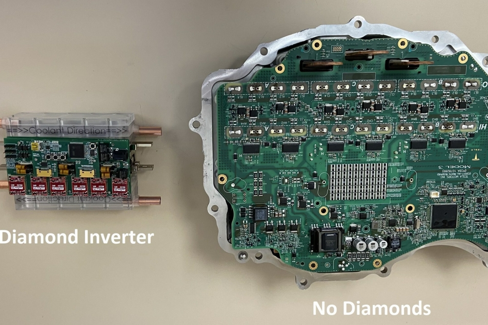
Diamond Foundry has created a 250W EV inverter based on its diamond wafer technology, with a power electronics unit six times smaller than that of a Tesla 3.

The company, which has its HQ in California, says the solution also delivers power more efficiently, thanks to a smart design enabled by diamond wafers in composition with established SiC dies.

Overall, the new 250W DF Perseus inverter use 18 SiC chips, occupies a volume of 0.46 litres and has a power density of 500KW/L In comparison, a Tesla 3 inverter has 96 SiC chips, occupies 28 litres, and has a power density of 9KW/L.

Power semiconductor design is driven by thermal conductivity ( the path to cool them dow) and electrical conductivity (the path to carry high currents). The thermal path has always been a challenge. To add to the problem, power semiconductors need to be isolated because of the high voltages – and voltage isolation barriers have poor thermal conductivity.

The company says that advent of cost efficient diamond wafers overcomes these issues by enabling extreme thermal performance plus extreme electrical insulation.

QD company Quantum Science expands into new facility
Innoscience files lawsuit against Infineon
Riber revenues up 5% to €41.2m
Forvia Hella to use CoolSiC for next generation charging
Photon Design to exhibit QD simulation tool
Ortel transfers CW laser fabrication to Canada
Luminus adds red and blue multi-mode Lasers
PseudolithIC raises $6M for heterogeneous chiplet tech
Mesa sidewall design improves HV DUV LEDs
IQE revenue to exceed expectations
'Game-changing' VCSEL system targets clinical imaging
German start-up secures finance for SiC processing tech
Macom signs preliminaries for CHIPS Act funding
IQE and Quintessent partner on QD lasers for AI
EU funds perovskite tandems for fuel-free space propulsion
EU to invest €3m in GeSi quantum project
Transforming the current density of AlN Schottky barrier diodes
Turbocharging the GaN MOSFET with a HfO₂ gate
Wolfspeed launches Gen 4 SiC MOSFET technology
Report predicts high growth for UK's North East
Element Six unveils Cu-diamond composite
SemiQ launches hi-rel 1700V SiC MOSFETs
Lynred to exhibit Eyesential SWIR sensor for machine vision
Thorlabs buys VCSEL firm Praevium Research
Advancing tuneable InP lasers on a heterogeneous platform
P-GaN gate HEMTs have record threshold voltage
Guerrilla RF releases GaN power amplifier dice
Narrow-linewidth DFB lasers now at 405 and 488nm
Researchers develop tech for future fast-charging stations
Vermont GaN Tech Hub awarded nearly $24M
Onsemi completes buy-out of Qorvo SiC JFET business
Quantum Science announces Innovate UK funding
×
Search the news archive

To close this popup you can press escape or click the close icon.
Logo
x
Logo
×
Register - Step 1

You may choose to subscribe to the Compound Semiconductor Magazine, the Compound Semiconductor Newsletter, or both. You may also request additional information if required, before submitting your application.


Please subscribe me to:


You chose the industry type of "Other"

Please enter the industry that you work in: