Loading...
News Article

OKI develops GaN lift off/bonding technology

News

Development paves the way to high current vertical GaN power devices

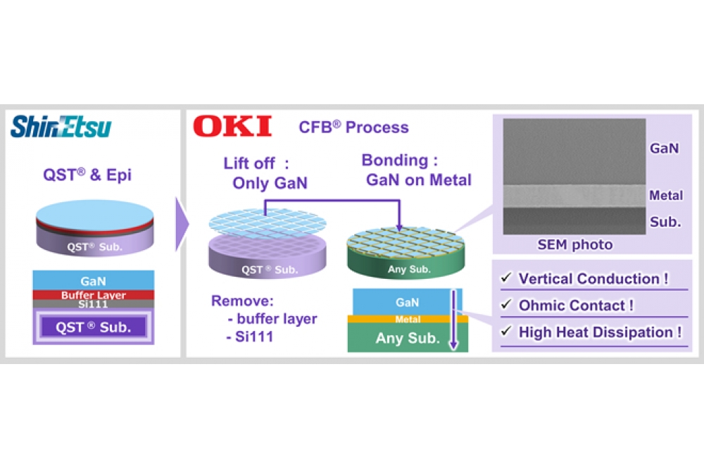
Japanese firm OKI, in collaboration with Shin-Etsu Chemical has announced the successful development of a technology that uses OKI's CFB (crystal film bonding) technology to lift off only the GaN functional layer from Shin-Etsu Chemical's QST (Qromis Substrate Technology) and bond it to a different material substrate.

The companies say this technology enables the vertical conduction of GaN and is expected to contribute to the realisation and commercialisation of vertical GaN power devices capable of controlling large currents.

The coefficient of thermal expansion of Shin-Etsu Chemical's QST substrate is equivalent to that of GaN. This means it can suppress warpage and cracking. It also enables the crystal growth of thick GaN films with high breakdown voltages even on wafers larger than 8 inches, enabling the production of wafers with larger diameters.

OKI's CFB technology can lift off only the GaN functional layer from the QST substrate while maintaining high device characteristics. The insulating buffer layer required for GaN crystal growth can be removed and bonded to various substrates via metal electrodes that allow ohmic contact. Bonding of these functional layers to a conductive substrate with high heat dissipation will enable both high heat dissipation and vertical conductivity, according to OKI.

In the future, the two companies aim to develop vertical GaN power devices through Shin-Etsu Chemical's provision of QST substrates or GaN grown QST substrates to companies manufacturing GaN devices, and OKI's provision of CFB technology through partnering and licensing.

OKI also hopes to use CFB technology to provide added value to semiconductor devices that go beyond the framework of single materials.

Mitsubishi joins Horizon Europe's FLAGCHIP project
Vishay launches new high voltage SiC diodes
UK team leads diamond-FET breakthrough
GaN adoption at tipping point, says Infineon
BluGlass files tuneable GaN laser patents
QD company Quantum Science expands into new facility
Innoscience files lawsuit against Infineon
Riber revenues up 5% to €41.2m
Forvia Hella to use CoolSiC for next generation charging
Photon Design to exhibit QD simulation tool
Ortel transfers CW laser fabrication to Canada
Luminus adds red and blue multi-mode Lasers
PseudolithIC raises $6M for heterogeneous chiplet tech
Mesa sidewall design improves HV DUV LEDs
IQE revenue to exceed expectations
'Game-changing' VCSEL system targets clinical imaging
German start-up secures finance for SiC processing tech
Macom signs preliminaries for CHIPS Act funding
IQE and Quintessent partner on QD lasers for AI
EU funds perovskite tandems for fuel-free space propulsion
EU to invest €3m in GeSi quantum project
Transforming the current density of AlN Schottky barrier diodes
Turbocharging the GaN MOSFET with a HfO₂ gate
Wolfspeed launches Gen 4 SiC MOSFET technology
Report predicts high growth for UK's North East
Element Six unveils Cu-diamond composite
SemiQ launches hi-rel 1700V SiC MOSFETs
Lynred to exhibit Eyesential SWIR sensor for machine vision
Thorlabs buys VCSEL firm Praevium Research
Advancing tuneable InP lasers on a heterogeneous platform
P-GaN gate HEMTs have record threshold voltage
Guerrilla RF releases GaN power amplifier dice
×
Search the news archive

To close this popup you can press escape or click the close icon.
Logo
x
Logo
×
Register - Step 1

You may choose to subscribe to the Compound Semiconductor Magazine, the Compound Semiconductor Newsletter, or both. You may also request additional information if required, before submitting your application.


Please subscribe me to:


You chose the industry type of "Other"

Please enter the industry that you work in: