Loading...
News Article

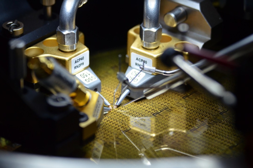
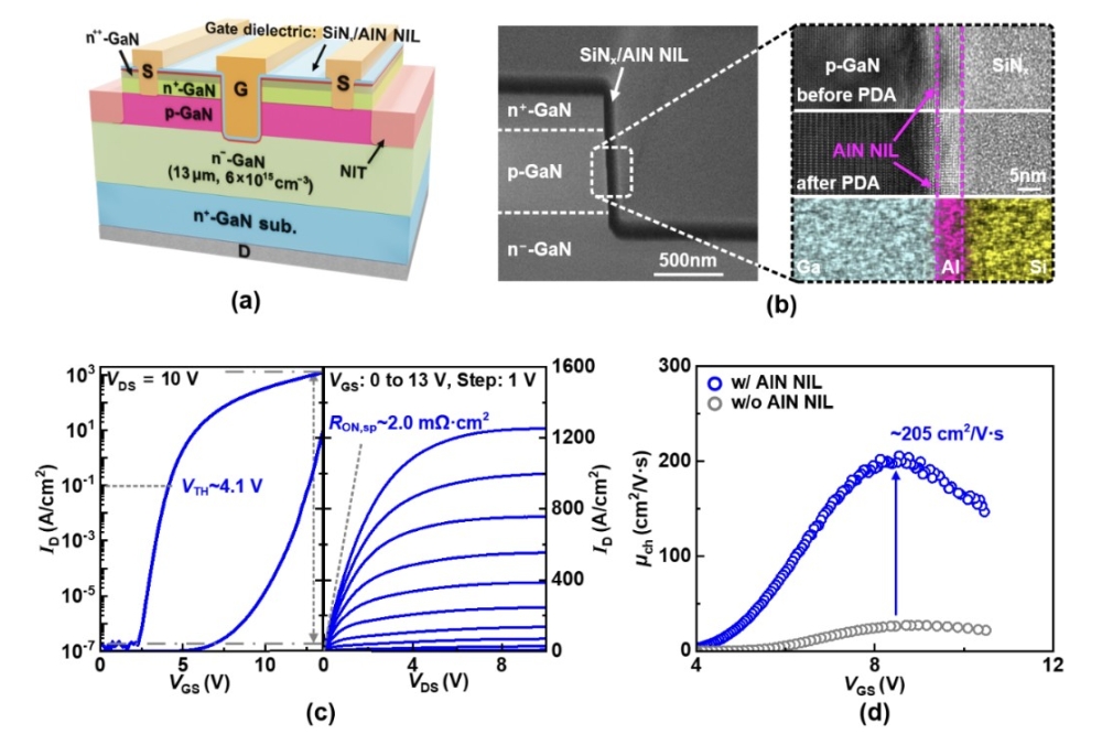
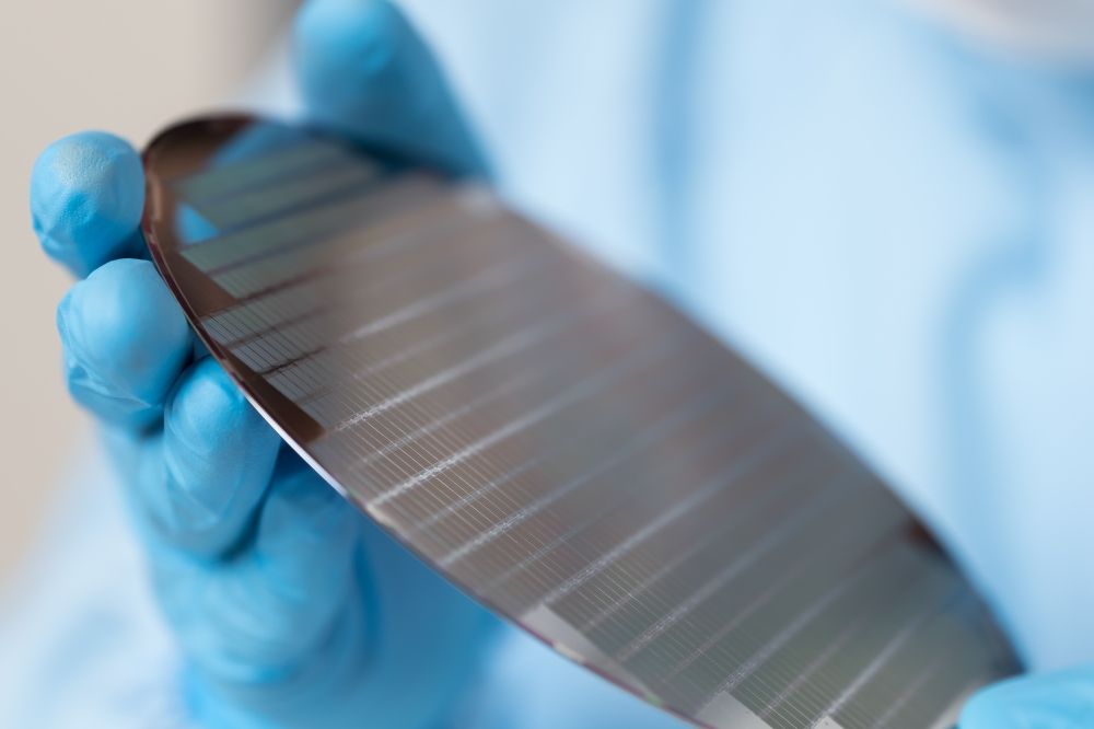
A*STAR and Centrotherm establish SiC partnership

News

Partners to combine IME's 200mm R&D SiC pilot line with Centrotherm’s tools to enhance the performance and reliability of SiC-based devices

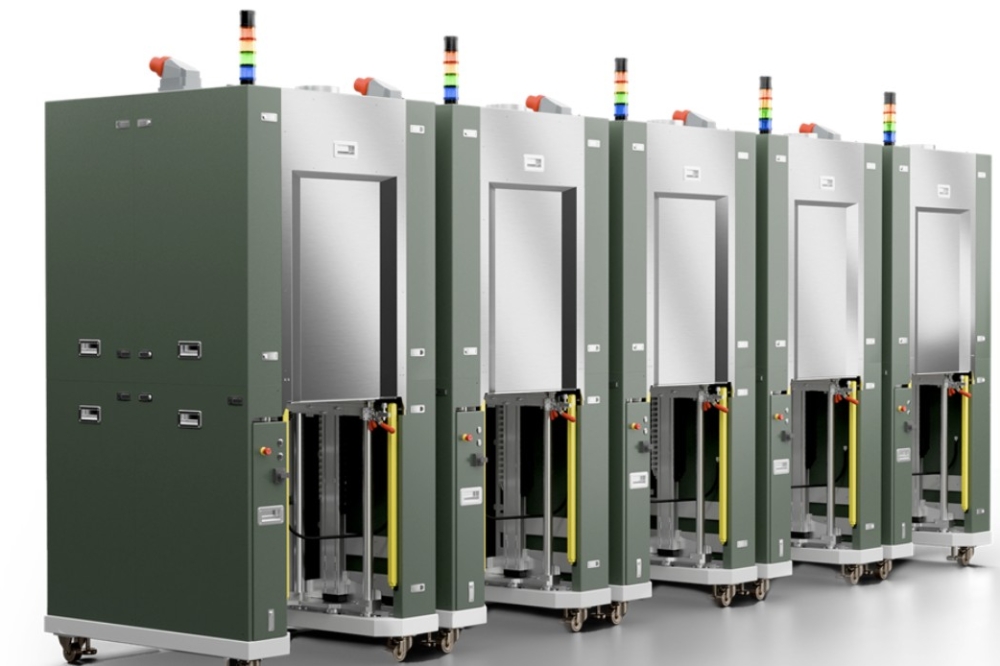
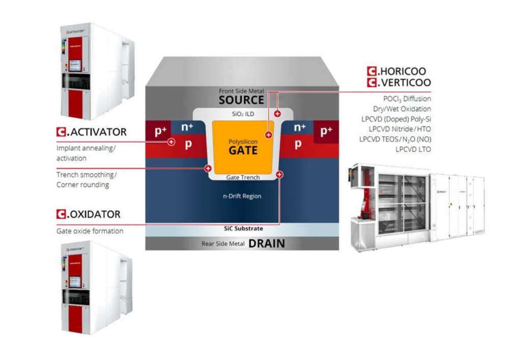
A*STAR Institute of Microelectronics’ (IME) and Centrotherm have embarked on a partnership to advance SIC technology by combining IME's 200mm open R&D SiC pilot line with Centrotherm’s diffusion and annealing tools.

The collaboration aims to build on IME’s process integration and device characterisation capabilities and Centrotherm’s specialised tools to develop thermal processes for SiC-based device fabrication, such as optimising trench and gate oxide formation. The aim is to enhance the performance and reliability of SiC-based devices such as MOSFETs and diodes. As part of the partnership, Centrotherm will establish a dedicated technology team in Singapore to offer technological know-how, process recipes, and on-site support.

“We look forward to advance SiC technology through our partnership with Centrotherm. Through the combination of IME's 200mm SiC R&D pilot line with Centrotherm’s advanced tools, we can accelerate R&D to better address the industry’s needs,” said Terence Gan, executive director of A*STAR’s IME.

“This collaboration between IME and Centrotherm marks an exciting chapter in the world of SiC technology. The shared vision, expertise and resources of both organisations promise to drive innovation, elevate industry standards and foster local growth in the field of semiconductor manufacturing. As we move towards the future of SiC and power electronics, we plan to further enhance diffusion and annealing specialisation in wide-bandgap process modules and expand expertise into SiC, GaN, and other innovative wide-bandgap materials,” said Helge Haverkamp, CTO of Centrotherm.

Finwave signs distribution agreement with RFMW
USTC team develops GaN nanowire 'synapse'
Violumas announces ultra-narrow beam UV LED
MoS₂ offers new way to detect signals in cells
CSA Catapult hosts roundtable on UK strategy and growth
High inversion channel mobility in 1.4 kV vertical GaN MIS-FET
ST, MICROOLED and Quanta to deliver AR glasses design
$25b compound semi market by 2030
Coating stops QDs blinking and fading
Unleashing the potential of the JFET
Aixtron hits targets despite challenging market
Rohm launches 650V GaN HEMT in TOLL package
New kind of FET uses 'incipient' ferroelectricity'
Penn State to establish advanced semiconductor lab
Ex Ams Osram CEO to become Aixtron chair
Boosting electro-optic performance in AlScN
Silanna UV launches water dispenser disinfection tech
UK SiC fab secures Indian investment
Navitas releases Q4 and FY results
TekSiC Xforge PVT targets next gen SiC crystal growth
U-M wins up to $7.5m for heat-tolerant SiC project
Perovskite PVs: thermal stress is the key to stability
SounDigital uses CoolGaN to boost sound quality
Ennostar merges subsidiaries Epistar and Lextar
BluGlass gets repeat order for GaN laser bars
SemiQ announces three new 1200V SiC full-bridge modules
Korean team develops method to evaluate SiC chips for space
CGD secures $32m in funding
Next gen solar cells can be totally recyclable
Sivers appoints Alexander McCann as senior advisor
Infineon tackles GaN package standards
Frontgrade qualifies Class L GaN DC-DC and EMI filter
×
Search the news archive

To close this popup you can press escape or click the close icon.
Logo
x
Logo
×
Register - Step 1

You may choose to subscribe to the Compound Semiconductor Magazine, the Compound Semiconductor Newsletter, or both. You may also request additional information if required, before submitting your application.


Please subscribe me to:


You chose the industry type of "Other"

Please enter the industry that you work in: