Penn State to establish advanced semiconductor lab
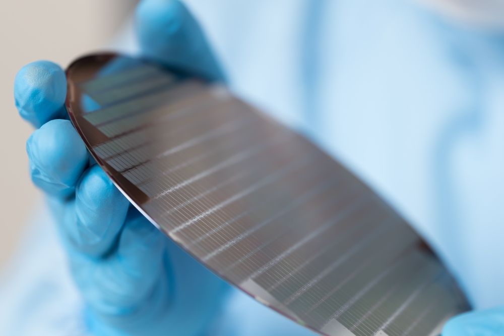
Penn State University's R&D capabilities in next-generation compound semiconductor technology will benefit from $4.3 million in infrastructure funding and in-kind support through membership of MMEC, a consortium of regional partners focused on microelectronics research and development.
The funding from MMEC, part of a broader initiative under the US DoD Microelectronics Commons effort under the CHIPS Act, will help the University establish a lab for semiconductor thin films and device research in the Materials Research Institute’s (MRI) facilities.
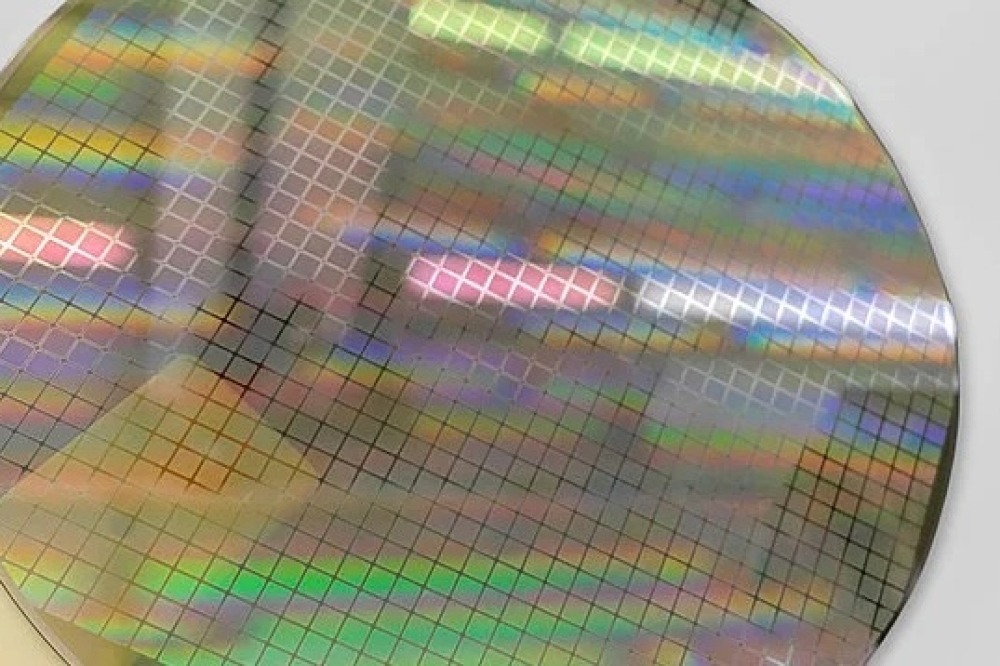
At the heart of the new facility will be an MOCVD tool, manufactured by Aixtron, which will enable the deposition of semiconductor thin films on multiple wafers at a time at sizes up to four-inch diameter. The tool is unique in its ability to grow both wide bandgap semiconductors such as GaN and 2D materials.
“This tool will allow students and early career researchers to gain hands-on experience with state-of-the-art thin film deposition equipment used by industry for compound semiconductor thin film manufacturing,” said Joan Redwing, lead investigator on the infrastructure project and distinguished professor of materials science and engineering and director of MRI’s Two-Dimensional Crystal Consortium.
In addition to the MOCVD tool, the lab will house several other specialised instruments. One is a Jupiter XR atomic force microscope from Oxford Instruments Asylum Research for fast scanning and full-wafer mapping, which will help enhance quality control and characterisation of thin film materials.
The other is an evaporator for deposition of specialised contact metal stacks for devices fabricated using 2D materials. This tool will support research by Suzanne Mohney, professor of materials science and engineering, and Saptarshi Das, professor of engineering science and mechanics, in addition to other faculty.
The equipment will be available for use by researchers inside and outside Penn State as a user facility with shared process know-how. The lab’s capabilities will provide opportunities for a range of Penn State researchers, including faculty working on power electronics and 2D-device development.

