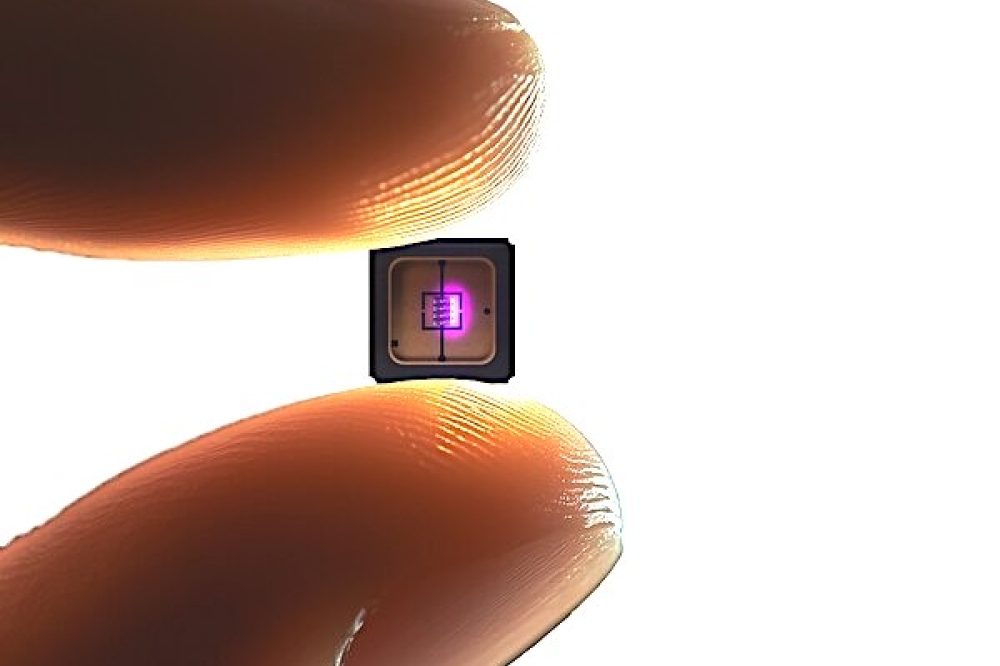
Study unlocks perovskite's nanoscale secrets
Research reveals how to tune surface properties to optimise efficiency and better control degradation
In their efficiency at converting sunlight to electricity, perovskites are becoming comparable to silicon. But one big remaining drawback is longevity: They tend to break down in a matter of months to years, while silicon solar panels can last more than two decades. And their efficiency over large module areas still lags behind silicon.
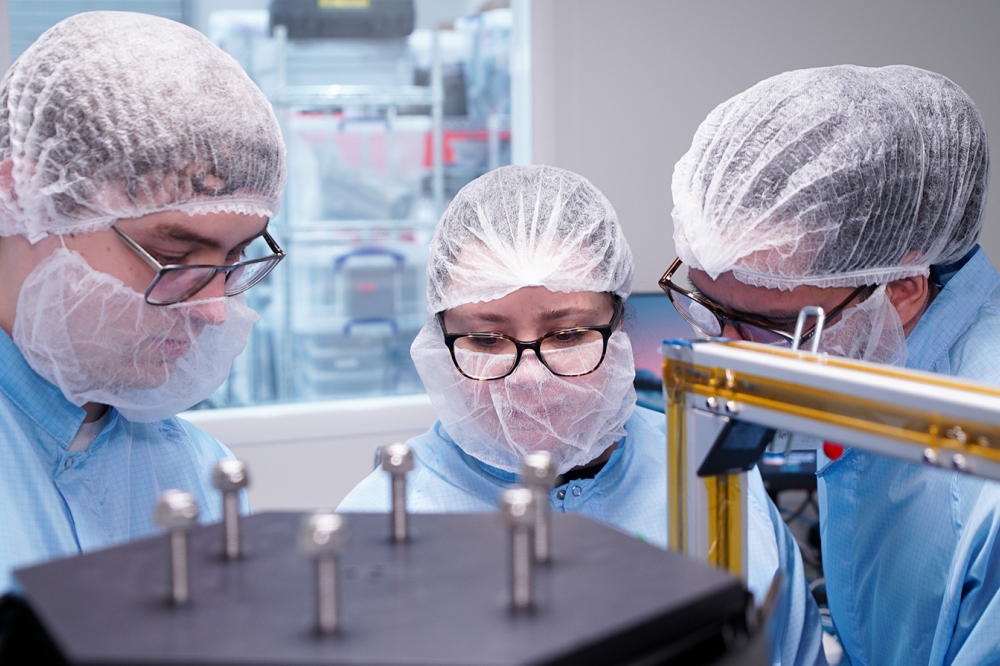
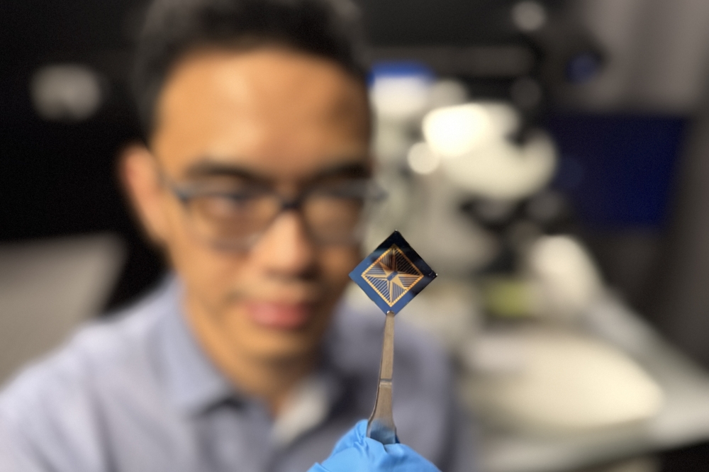
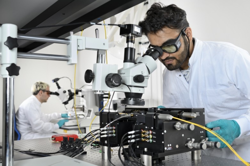
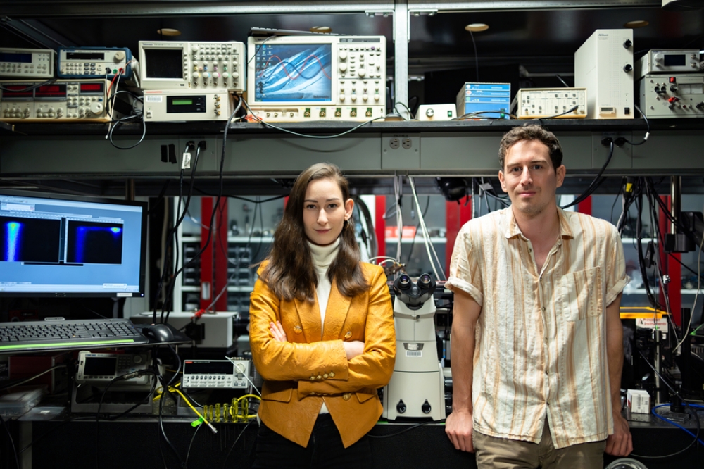
Now, a team of researchers at MIT (including Madeleine Laitz and Dane deQuilettes pictured above) along with researchers at the Korea Research Institute of Chemical Technology, Cambridge University, the University of Washington in Seattle, and Sungkyunkwan University in Korea, has revealed ways to optimise efficiency and better control degradation, by engineering the nanoscale structure of perovskite devices.
The study reveals new insights on how to make high-efficiency perovskite solar cells, and also provides new directions for engineers working to bring these solar cells to the commercial marketplace.
The work is described in the journal Nature Energy, in the paper 'Reduced recombination via tunable surface fields in perovskite thin films'. Authors include Dane deQuilettes, a recent MIT postdoc who is now co-founder and chief science officer of the MIT spinout Optigon, along with MIT professors Vladimir Bulovic and Moungi Bawendi, and ten others at MIT and in Washington state, the UK, and Korea.
“Ten years ago, if you had asked us what would be the ultimate solution to the rapid development of solar technologies, the answer would have been something that works as well as silicon but whose manufacturing is much simpler,” Bulovic says. “And before we knew it, the field of perovskite photovoltaics appeared. They were as efficient as silicon, and they were as easy to paint on as it is to paint on a piece of paper. The result was tremendous excitement in the field.”
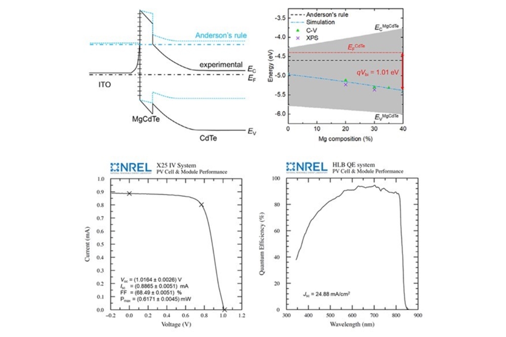
The new study looks at a very small but key detail: how to “passivate” the material’s surface, changing its properties in such a way that the perovskite no longer degrades so rapidly or loses efficiency. “The key is identifying the chemistry of the interfaces, the place where the perovskite meets other materials,” Bulovic says.
Engineers have developed methods for passivation, for example by using a solution that creates a thin passivating coating. But they’ve lacked a detailed understanding of how this process works — which is essential to make further progress in finding better coatings.
The team has looked at the interfaces between the perovskite layer and other materials, and how they develop, in unprecedented detail. This close examination of the passivation coating process and its effects resulted in “the clearest roadmap as of yet of what we can do to fine-tune the energy alignment at the interfaces of perovskites and neighbouring materials,” and thus improve their overall performance, Bulovic says.
While the bulk of a perovskite material is in the form of a perfectly ordered crystalline lattice of atoms, this order breaks down at the surface. There may be extra atoms sticking out or vacancies where atoms are missing, and these defects cause losses in the material’s efficiency. That’s where the need for passivation comes in.
“This paper is essentially revealing a guidebook for how to tune surfaces, where a lot of these defects are, to make sure that energy is not lost at surfaces,” deQuilettes says. “This is the first paper that demonstrates how to systematically control and engineer surface fields in perovskites.”
The common passivation method is to bathe the surface in hexylammonium bromide, a technique developed at MIT several years ago by Jason Jungwan Yoo, who is a co-author of this paper, that led to multiple new world-record efficiencies. By doing that “you form a very thin layer on top of your defective surface, and that thin layer actually passivates a lot of the defects really well,” deQuilettes says. “And then the bromine, which is part of the salt, actually penetrates into the three-dimensional layer in a controllable way.” That penetration helps to prevent electrons from losing energy to defects at the surface.
These two effects, produced by a single processing step, produces the two beneficial changes simultaneously. The passivation reduces the energy loss of electrons at the surface after they have been knocked loose by sunlight. These losses reduce the overall efficiency of the conversion of sunlight to electricity, so reducing the losses boosts the net efficiency of the cells.
That could rapidly lead to improvements in the materials’ efficiency in converting sunlight to electricity, he says. The recent efficiency records for a single perovskite layer, several of them set at MIT, have ranged from about 24 to 26 percent, while the maximum theoretical efficiency that could be reached is about 30 percent, according to deQuilettes.
“In the silicon photovoltaic industry, if you’re gaining half of a percent in efficiency, that’s worth hundreds of millions of dollars on the global market,” he says. A recent shift in silicon cell design, essentially adding a thin passivating layer and changing the doping profile, provides an efficiency gain of about half of a percent. As a result, “the whole industry is shifting and rapidly trying to push to get there.” The overall efficiency of silicon solar cells has only seen very small incremental improvements for the last 30 years, he says.
The record efficiencies for perovskites have mostly been set in controlled laboratory settings with small postage-stamp-size samples of the material. “Translating a record efficiency to commercial scale takes a long time,” deQuilettes says. “Another big hope is that with this understanding, people will be able to better engineer large areas to have these passivating effects.”
There are hundreds of different kinds of passivating salts and many different kinds of perovskites, so the basic understanding of the passivation process provided by this new work could help guide researchers to find even better combinations of materials, the researchers suggest. “There are so many different ways you could engineer the materials,” he says.
“I think we are on the doorstep of the first practical demonstrations of perovskites in the commercial applications,” Bulovic says. “And those first applications will be a far cry from what we’ll be able to do a few years from now.” He adds that perovskites “should not be seen as a displacement of silicon photovoltaics. It should be seen as an augmentation — yet another way to bring about more rapid deployment of solar electricity.”
The work was supported by the Tata Trust, the MIT Institute for Soldier Nanotechnologies, the US Department of Energy, and the US National Science Foundation.