An innovative approach to doping challenges
Doping limitations, either p-type or n-type, in many compound semiconductors, such as p-type doping in CdTe and GaN, and n-type doping in ZnTe, have been a long-standing challenge. This is because of fundamental material properties such as large effective masses and small effective dielectric constants.
Now researchers at Arizona State University (ASU) led by Yong-Hang Zhang have invented a novel approach to circumvent doping challenges, using interface states and charge transfer effects to tailor Fermi level without the use of any p-type materials in CdTe solar cells.
Their paper 'Interface Fermi-level engineering for selective hole extraction without p-type doping in CdTe solar cells to reach high open circuit voltage (>1 V)' is published in the Wiley journal Solar RRL.
For decades, the inability to reliably achieve high hole concentrations in CdTe has limited the open-circuit voltage (Voc) and thus capped device performance. By demonstrating a Voc exceeding 1 V in an architecture without p-type doping, this study establishes a paradigm shift for CdTe solar cell design, according to the researchers.
More importantly, it introduces a concept that could be revolutionary for existing CdTe manufacturing lines — enabling higher efficiency and thermal stability without fundamentally altering the absorbing material growth process or requiring complex doping schemes.
In previous work, the same ASU team used a p-type amorphous silicon (a-Si:H) layer as the hole-selective contact, i.e. 'remote junction' idea, in CdTe/MgCdTe double-heterostructure (DH) solar cells to achieve a record Voc of 1.1 V, and active-area efficiency of 20 percent.
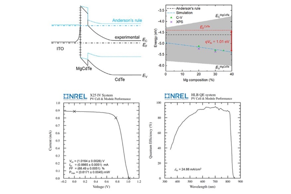
However, that design still relied on p-type materials a-Si:H, which is not stable in air without annealing. In contrast, the current device architecture features only n-type layers — including the absorber and the transparent contact — and achieves much improved reliability and similar Voc exceeding 1 V.
Zhang’s collaborators, Jack Ma’s team at University of Wisconsin–Madison have confirmed the Fermi-level engineering at the ITO/(Mg)CdTe interface using X-ray photoelectron spectroscopy (XPS) measurements.
The devices were fabricated using high-quality monocrystalline CdTe/MgCdTe DH grown by molecular beam epitaxy. A transparent conductive ITO layer was sputtered on top to serve as the front contact. Structural characterisation confirmed excellent crystalline quality and smooth interfaces. Additionally, advanced XPS techniques were employed to validate the interfacial band alignment and support the interfacial Fermi-level engineering concept.
The US National Renewable Energy Laboratory (NREL) has confirmed a Voc exceeding 1 V and efficient carrier collection of the device, demonstrating the effectiveness of the all-n-type design.
For the future, the researchers say that the same Fermi-level engineering approach can be readily extended to other semiconductors with doping issues, such as III-nitrides, oxides, diamond, HgCdTe etc.