CS Mantech: Improving the capabilities of RF GaN

Options for building better HEMTs including switching the polarity, introducing InAlN barriers and optimising buffer growth.
BY RICHARD STEVENSON, EDITOR, CS MAGAZINE
ΩAs a material for making compound semiconductor devices, GaN is peerless. It is an incredibly efficient light emitter, enabling a revolution in lighting, as well as the production of short-wavelength lasers that can read data off of discs and cut material. In addition, GaN has excellent electronic characteristics that are now being put to good use for improving the efficiency of chargers and power supplies.
With so many lucrative opportunities for GaN, one might overlook those that are not grabbing the headlines, but are still set to generate growing revenues over the coming years.
In that regard stands RF GaN, which is deployed in 4G and 5G base stations, radar and electronic warfare systems. According to market analyst Yole Group, sales of RF GaN devices for these applications are climbing, with total device revenue forecast to increase to $2 billion by 2029.
This market continues to attract investment to improve the performance of the GaN HEMT through changes to its architecture, its foundation and the epitaxial processes employed to produce this device. At this year’s CS Mantech, held in Tucson, Arizona, from 20-23 May, spokesmen for makers of devices, epiwafers and MOCVD tools all reported progress on these fronts. At this conference Sumitomo Electric Industries reported record-breaking output powers for N-polar HEMTs in the Ka-band, a partnership between Mitsubishi Electric and Furuno Electric unveiled a very efficient GaN HEMT for marine radar, WIN Semiconductors explained how an optimised buffer improves GaN HEMT linearity, and a European collaboration involving Aixtron discussed the use of depleted interfaces between the substrate and epilayers for minimising RF loss in GaN-on-silicon HEMTs.

Figure 1. Atomic force microscopy uncovers pits on the surface of III-polar HEMTs that can lead to device breakdown and current collapse (a). These pits are not observed in N-polar HEMTs.
Switching polarity
The GaN HEMTs that are winning commercial deployment feature an AlGaN buffer and a Ga-polar design. To improve performance, a number of researchers have considered refining this architecture. A team from the University of California, Santa Barbara, have enjoyed much success by turning to N-polar HEMTs, realising an output power density of 8.84 W mm-1 at 94 GHz, at a power-added efficiency of 27 percent. Meanwhile, at team from Fujitsu has delivered a power density of 3 W mm-1 at 96 GHz by replacing the conventional barrier with lattice matched InAlN.
At this year’s CS Mantech, Shigeki Yoshida from Sumitomo Electric Industries described efforts to combine both these valuable innovations. This team’s HEMTs, with an N-polar orientation and an InAlN barrier, are claimed to deliver a record-breaking power density of 12.8 W mm-1 at 28 GHz. Yoshida told Compound Semiconductor that in comparison, the output power of the company’s Ga-polar GaN HEMT product is about 4 W mm-1 in the Ka-band.
To produce their transistors, Yoshida and co-workers began by loading 100 mm semi-insulating SiC substrates into an MOCVD reactor and depositing a buffer layer, followed by an InAlN back barrier, an AlN spacer, a 12 nm-thick GaN channel and a GaN cap. On this epitaxial structure they added a HfSiOx gate insulator, selected for its high values for permittivity and breakdown field – they are 13 and 8.5 MV cm-1, respectively. To reduce source and drain contact resistance, the engineers introduced heavily doped n-type GaN selective growth regions. HEMTs were produced with a 200 mm gate length, a source-drain length of 2.5 µm, a gate-source length of 0.9 µm, and a gate-drain length of 1.4 µm.

Figure 2. Engineers at Sumitomo Electric Industries have benchmarked
their N-polar GaN/InGaN HEMTs (blue star) against N-polar GaN/AlGaN
HEMTs.
On-wafer measurements determined an electron mobility of 928 cm2 V-1 s-1 and a surface roughness, according to atomic force microscopy, of 0.304 nm – that’s the root-mean-square roughness over a 1 µm by 1 µm area. This value for roughness is lower than that for III-polar GaN HEMTs, suggesting a suppression of electron scattering and a high electron mobility. For the surface of the III-polar GaN HEMTs, pits are seen on the surface that can cause device breakdown and current collapse (see Figure 1). Note that these imperfections are not seen on the surface of the team’s N-polar HEMTs.
One of the benefits of the N-polar HEMT over its conventional cousin is that the external electric field resulting from the gate voltage and the internal electric field due to the polarisation of the barrier are in opposite directions, rather than the same direction. This allows N-polar HEMTs to have a higher breakdown voltage, with Yoshida and co-workers estimating a breakdown voltage of more than 60 V, based on electrical measurements.

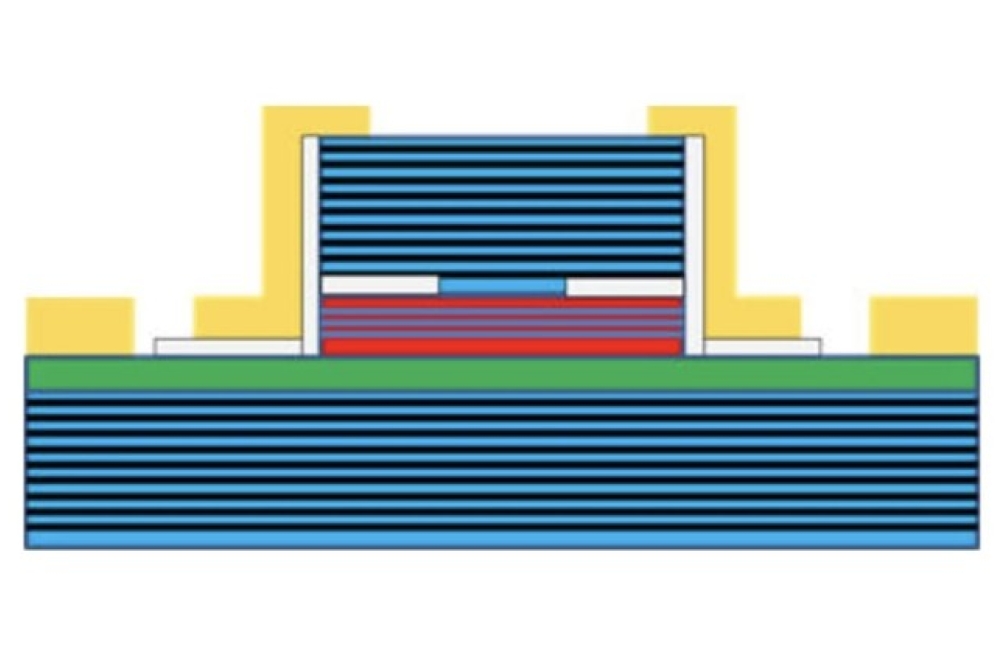
Figure 3. For HEMTs produced by Mitsubishi Electric and Furuno Electric,
the length of the source-connected field plate (Lsfp) impacts the
power-added efficiency (PAE), and the ratio of pulsed-to-DC current,
which provides a measure of current collapse. The PAE is measured at a
9.6 GHz.
Additional measurements on this device have determined a maximum drain current density of 2.64 A mm-1, a current gain cut-off frequency (ft) of 30 GHz, and a maximum oscillation frequency (fmax) of 96 GHz.
The saturated output power for the device, 12.8 W mm-1 for 28 GHz load-pull power sweeps, is claimed to be the highest value ever reported for N-polar HEMTs in the Ka-band (see Figure 2). The team argues that this output power is limited by impedance tuning.
“We have to design and fabricate pre-matching circuits to improve [impedance tuning],” remarked Yoshida. However, that’s not the next plan – it is to develop an AlN buffer to improve heat dissipation.
Marine radar
For GaN HEMTs for radar, the opportunities that are most often discussed are associated with defence and aviation. But there is also the option to deploy these wide bandgap devices on ships, where they can displace vacuum electron devices, such as magnetrons. Merits of GaN over the vacuum-tube-based incumbents include reductions in size and weight, a longer life and a hot-start source. The extension in lifetime is substantial, with magnetrons needing to be replaced every 5,000 hours, while GaN HEMTs have a mean-time-to-failure of over 1,000,000 hours. Another merit of the latter is that it is compatible with Doppler analysis – this ensures safe navigation by enabling the tracking of vessels and floating wreckages.
Speaking about this opportunity at this year’s CS International, Eiji Yagyu from Mitsubishi Electric described the development of X-band to Ka-band GaN HEMTs with a high power-added efficiency. These transistors can be used to produce a marine radar with a range of 96 nautical miles.

Figure 4. RF power characteristics of GaN-on-SiC HEMTs (a) and GaN-on-GaN HEMTs (b) at 2.4 GHz. The total gate width is 0.2 µm.
This programme has involved the production of AlGaN/GaN HEMTs on SiC substrates with a gate length of 0.2 µm using what are claimed to be reliable structures and techniques. These HEMTs incorporate an iron-doped buffer layer, their fabrication involves ion-implanted isolation, and they feature a silicon-implanted ohmic contact region, a T-shaped gate and a source-connected field plate. According to the team, although these devices are ordinary HEMTs, to ensure a high power-added efficiency and reliability, they have optimised the fabrication processes, the epitaxial layers, and the electrode layout and design.
Measurements of these HEMTs reveal that there is a sweet spot for the power-added efficiency. Efficiency hits 77.8 percent at 9.6 GHz when the length for the source-connected field plate is 0.6 µm (see Figure 1). The current collapse, evaluated by the ratio of the pulsed-to-DC current, improves with the length of the field plate, but saturates at 0.6 mm. The team also notes that plots of pulsed and DC current reveal that traps working at a semi-on bias play a dominant role in determining efficiency.
Yagyu and co-workers have used their HEMTs to develop MMIC PAs. They have also made an X-band GaN HEMT with a total gate width of 29.6 mm that produces 200 W in the X-band, and they have developed an internally-matched FET PA using GaN die and input/output networks with non-uniform comb lines. The PA produces an RF output power of 240 W at a power-added efficiency of 51 percent. By combining two die, the team have produced a PA with an output power of 467 W and a power-added efficiency of 46 percent.

Figure 5. Transfer characteristics of HEMTs made by WIN Semiconductor
reveal that the introduction of a new process has increased the dynamic
range of this device.
The solid-state PA produced by the team, delivering 200 W, is said to be equivalent to a 25 kW magnetron, but reduces power consumption from 71 W to 27 W. The frequency deviation of the solid-state PA is 0.15 MHz, 40 times smaller than that of the magnetron, and phase deviation is lower by more than a factor of 100. The combination of high-frequency stability and a low phase noise makes the radar based on GaN HEMTs far better suited to Doppler analysis.
The team have also started to investigate the potential of GaN-on-GaN HEMTs, which they argue could reduce power consumption and cost. Yagyu told Compound Semiconductor that although GaN substrates are currently more expensive than those made from SiC, this could change. “GaN has the possibility of a lower price than SiC, because large GaN ingots could be rapidly grown from the liquid-phase like silicon,” argued Yagku, adding that SiC substrates are grown from the vapour phase.
Investigations on the use of GaN have begun by comparing the density of threading dislocations on GaN-on-SiC and GaN-on-GaN by counting etch pits. For GaN-on-GaN, this approach gave a figure of 3 x 10⁶ counts cm-3, more than 200 times lower than that for GaN-on-SiC. This led the team to reason that growth on native GaN will reduce the trapping of electrons and current collapse, and improve the power and linearity of amplification.
These engineers have produced two-finger HEMTs with a gate length of 1 µm on 15 mm by 15 mm substrates of GaN and SiC, and compared the performance of these two types of device. Using the ratio of pulsed-to-DC current to evaluate current collapse, the team observed steep degradation for transistors grown on SiC, and no significant degradation for those with a native foundation.
To evaluate linearity, Yagku and co-workers considered third-order intermodulation distortion, using a centre frequency of 2.4 GHz and a spacing frequency of 2 MHz. This investigation confirmed a smaller distortion for HEMTs grown on GaN than those on SiC. The output power is also higher for HEMTs on a native substrate (see Figure 4).
Plans for Yagku and co-workers include investigating the best design of GaN-on-GaN, and demonstrating this choice of materials in other microwave applications. “As GaN-on-GaN has less-distortion in modulated signals than GaN-on-SiC, I will demonstrate this superiority in applications,” remarked Yagku.

Figure 6. WIN Semiconductor’s newly developed HEMT has a higher output
power than its conventional equivalent, according to 3.6 GHz pulsed
load-pull measurements. Each data point represents an output power
(Pout) at 3 dB compression and a drain efficiency at a different output
impedance.
Suppressing memory effects
One of the downsides of the GaN HEMT is a memory effect that is induced by a drift in the bias current – that’s the current flowing in the drain when there is DC bias and RF signal applied to the input. The memory effect degrades device performance, causing variations in gain and signal distortion. Due to this, when GaN HEMTs are used in mobile communication infrastructure, there’s a need for a digital predistortion model that compensates for the memory effect. The addition of this model increases computational complexity.
To suppress this memory effect, Wayne Lin and colleagues at WIN Semiconductors have optimised buffer growth, replacing an iron-doped buffer with one that’s produced with an undisclosed process, which is starting to be used in products shipped to customers.
At CS Mantech Lin presented proof of the superiority of the new process by comparing the performance of HEMTs formed on SiC that are produced using this approach with those made in a conventional way. To produce the control, the engineers at WIN grew an iron-doped GaN buffer on SiC by MOCVD, followed by a GaN channel, an AlGaN barrier and a GaN cap. The alternative has an optimised buffer. The only other difference from the control is an AlN spacer layer, inserted between the GaN channel and AlGaN barrier.
The purpose of the AlN spacer is to increase the concentration of the two-dimensional electron gas. Lin told Compound Semiconductor that this spacer does not improve the linearity of the HEMT.
When asked if the spacer has any downsides, Lin remarked: “So far, so good.” He added that WIN will collect statistical data to check if the new buffer has any drawbacks.
Fabrication of WIN’s HEMTs involved defining the ohmic metal by optical lithography, followed by electron-beam evaporation of Ti/Al/Ni/Au stacks. Annealing formed the ohmic contact, before the addition of a first SiN passivation layer. After etching a gate opening, the team added a Schottky gate by evaporating Ni/Pd/Au, before depositing a second SiN layer that sits between the gate metal and a source-coupled field plate. To complete the fabrication process, the engineers added a SiN layer to protect the surface, and introduced two metal interconnection layers to enhance the HEMT’s current-handling capability.
Plotting the drain current as a function of gate voltage revealed an increase in turn-on voltage for HEMTs produced with the new process (see Figure 5). This increase, which expands the dynamic range of the device, is attributed to the AlN spacer layer.
To investigate large signal performance, Lin and co-workers undertook 3.5 GHz pulsed load-pull measurements on a 10 x 125 mm device, using a drain current for what is described as deep class AB operation, and a drain voltage of 50 V, suitable for base station applications. The output power density for the design with the new buffer exceeds that of the control, delivering more than 12 W mm-1 (see Figure 6).
Insights into the drift in the bias current have come from measuring the transient waveform of this current in a pulsed load-pull system with a current probe. These measurements, using 36 ms pulsed RF signal excitation, reveal strong current collapse in the HEMT with the iron-doped buffer. In comparison, the HEMT with the new buffer technology has a 60 percent reduction in bias current drift and a quick recovery time.
To evaluate intermodulation distortion of RF PAs, the engineers at WIN have determined the ratio of the main channel power to that of adjacent channels. These measurements show a generally better performance for the newly developed HEMT, indicating superior linearity.
WIN has started to offer its new process to selected customers. A full release is planned during the last quarter of this year.
Minimising RF loss
For RF applications, growing the device on a silicon substrate has much appeal in terms of cost. However, SiC is easier to work with, as it offers smaller differences in lattice constant and thermal expansion coefficient with the epilayers, as well as a lower electrical conductivity. The latter strength, stemming from the wider bandgap, is a significant asset, as a lower conductivity cuts RF loss, which degrades the quality factor of passive components, the efficiency of the PA, and the linearity of switches.
To improve the capability of GaN-on-silicon devices for 5G and 6G applications, a partnership between Aixtron, imec, KU Leuven and the Free University of Brussels has investigated the role of the thermal budget on the growth of GaN layers on silicon substrates. Epitaxial process parameters can influence the conductivity of the silicon substrate, due to the diffusion of aluminium and gallium into the substrate and changes to the interface between the AlN nucleation layer and the silicon substrate.
According to Aixtron’s Herwig Hahn, who spoke on behalf of the partnership at CS Mantech, the key finding of their investigation is that combining the leading MOCVD tool with state-of-the-art process know-how enables the use of GaN-on-silicon in applications where minimal RF loss is required.
The collaboration is convinced that a gallium/aluminium-free reactor is mandatory for minimising RF losses.
“An in-situ clean is key to enabling this,” said Hahn. “We recommend using either a G5+ C or G10-GaN to obtain minimal RF losses.”
Experiments involved in-situ cleaning with chlorine gas, followed by epitaxial growth on monocrystalline high-resistivity silicon that has been grown by the Czochralski method. On these substrates, which were prepared for growth by an oxide removal step under hydrogen gas at 1050 °C, the team undertook an aluminium pre-dose step at between 700 °C and 800 °C, followed by growth of AlN between 1000 °C and 1050 °C. In some cases they then deposited a range of epitaxial stacks.
During these studies, the team found that a low thermal budget could not guarantee the high resistivity that’s desired. Values can be as low as 800 Ω cm, which is well below substrate resistivity.
Increasing the pre-dose temperature from 700 °C to 800 °C produced a pronounced increase in resistivity. According to energy dispersive X-ray spectroscopy, a higher resistivity is associated the formation of a very thin SiN layer, and a SiC layer that occupies a significant part of the interfacial layer. Samplers with a lower resistivity just have a SiN layer at the interface.
Hahn and co-workers argue that predose optimisation of AlN-on-silicon slightly differs from that of a full GaN HEMT stack on silicon, and even a fully processed RF device. The researchers recommend full device processing and RF characterisation when optimising growth conditions.
The team have also considered co-planar waveguides in their study, obtaining resistivities above 10 kΩ cm with an optimised process, exceeding the value of 3.8 kΩ cm for a GaN-on-SiC reference sample.
According to these researchers, applying the optimised process to a full buffer stack will reduce resistivity, compared with that realised with a co-planar waveguide. However, they are confident that optimised epitaxial growth conditions will allow GaN-on-silicon HEMTs to enjoy a performance parity with their GaN-on-SiC cousins.
Hahn said that working with imec, those at Aixtron are continuing to optimise full GaN RF layer stacks, not only for 5G, but also for future-generation 6G applications. Such efforts will help to secure the future of GaN RF devices, throughout this decade and beyond.