Nexperia: Expanding GaN and SiC operations
Re-fitting its Hamburg fab is laying the foundations for Nexperia to hike its production of GaN and SiC transistors and diodes on 200 mm lines
Investing phenomenal sums in infrastructure that enables the production of SiC and GaN devices is the new norm. In this regard the likes of Infineon, Wolfspeed and Innoscience are making the biggest splashes, by building fabs of breath-taking proportions that are propelling their capacity for high-volume production of wide bandgap power devices.
But as well as constructing new fabs, chipmakers are spending a lot of money on repurposing the space within them for the manufacture of SiC and GaN diodes and transistors. And in this regard, Nexperia is not holding back – it’s investing $200 million in new tools and equipment to strengthen the development and production of its wide bandgap portfolio at its fab in Hamburg, Germany.
Nexperia has a tremendous pedigree in electronics, with a history going back 100 years, and second-generation parent companies that include the household name Philips. Production of vacuum tubes in Hamburg provided the first source of revenue in the 1920s, and in the decades that followed efforts extended to the research, development and production of semiconductor devices. Further milestones came in the 1980s and 1990s, including the first MOSFET and the first 150 mm line, respectively. And in this century, two of the biggest moves have been the carving out NXP from Philips in 2006, and in 2017, the spinning out of NXP’s standard product division under the name Nexperia.
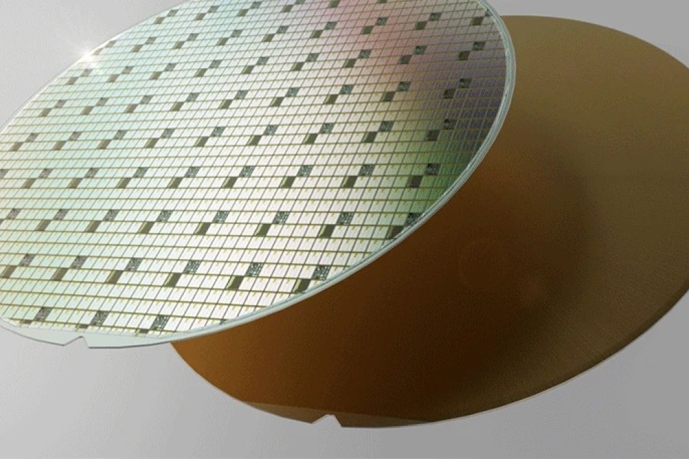
Today Nexperia is renowned as a major supplier of silicon power devices to automotive markets – this accounts for around half of its annual production of 100 billion discrete parts. However, over the last few years the power electronics producer has broadened its portfolio with the introduction of SiC and GaN devices.
Since 2019, GaN FETs have been part of this chipmakers’ line-up. SiC products came in 2023, and now include SiC diodes and SiC MOSFETs, the latter in collaboration with Mitsubishi Electric.
An additional advance came this June, with the introduction of the production lines for high-voltage GaN D-Mode transistors and SiC diodes at the Hamburg site. And according to Nexperia, the next milestone will be modern and cost-efficient 200 mm production lines for SiC MOSFETs and GaN HEMTs.
These new lines will be established over the next two-to-three years at the Hamburg facility that is undergoing substantial change, as all activities unrelated to either lab or fab are relocated to another office in the city. It’s a move that’s enabling an increase in the capacity of the silicon side of the business, as well as the expansion of SiC and GaN capability.
Nexperia’s Senior Director Product Management for SiC, Katrin Feurle, told Compound Semiconductor that most of the $200 million investment will be spent on new equipment and a remodelling of the fab to fit to the new machinery. Money is also allocated to increase the automation of existing infrastructure.
To scale epitaxial capabilities, Nexperia has placed orders with Aixtron. This German maker of MOCVD tools is a trusted partner that fulfils Nexperia’s needs, according to Carlos Castro, Vice President and General Manager for GaN.
As well as purchasing a range of processing tools to turn epiwafers into devices, Nexperia is making substantial investments in metrology.
Castro claims that Nexperia has a strong reputation for really high standards in production and performance, adding: “Metrology is key, because it gives you a very precise characterization and control of materials, structures, and the process.” In turn, this ensures performance, reliability, quality, and a competitive cost.
In addition to the equipment, Nexperia has recruited accompanying personal. “We have some people already on board there, experts in metrology,” says Castro.
This increase in headcount is part of a pattern of long-term growth in staff at the Hamburg site. In 2017 the facility had 950 employees, a figure that now stands at 1,600, with more than 50 added in the last three years for roles solely associated with wide bandgap devices.
Today, Nexperia is trying to fill another 20 positions. “But this is just the beginning of the journey,” says Feurle.

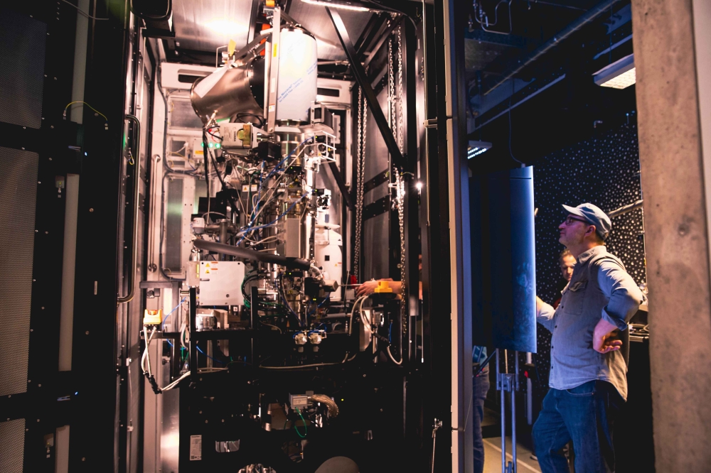
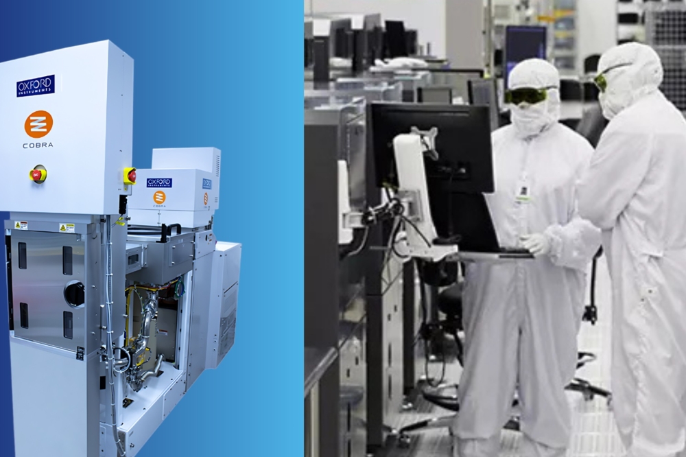
Lithography at Nexperia’s Hamburg Wafer-Fab
Growth in GaN…
Since launching its first wide bandgap power device in 2019, the GaN FET, Nexperia has made much progress with this class of transistor. Each new generation features a 20 percent cut in its specific on-resistance.
One of the strengths of Nexperia is that it supplies both E-mode and D-mode devices.
“We are the only supplier giving the option to customers to go for D-mode technology, which we believe is more suitable for high-voltage and high-power applications, as well for E-Mode devices, which are very successful right now in the market for low-voltage or low-power applications, like, for example, fast chargers for mobile phones or notebooks,” says Castro.
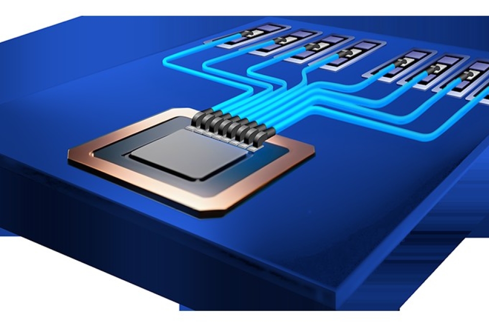
Another attribute of Nexperia’s GaN portfolio is that it draws on the company’s 20 years of expertise in copper clip technology. As well as ensuring a superior thermal performance, this packaging technology leads to better electrical performance, with a trimming of parasitics and stray inductance resulting in an increase in reliability. And that’s not all – the copper clip technology enables a much more compact design that ensures a higher efficiency, as well as the opportunity to turn to higher frequencies, a strength well suited to high-power applications, such as power supplies and electric vehicles.
While GaN power devices have much appeal, they are currently attracting bad press for patent battles fought between Innoscience and EPC and Infineon.
Castro is not expecting Nexperia to be on the wrong side of such skirmishes, since it has its own IP. Back in 2017 and 2018 the company worked with a collaborator in the US, an activity that involved some licensing, and since then it has been internally and significantly growing its IP portfolio.

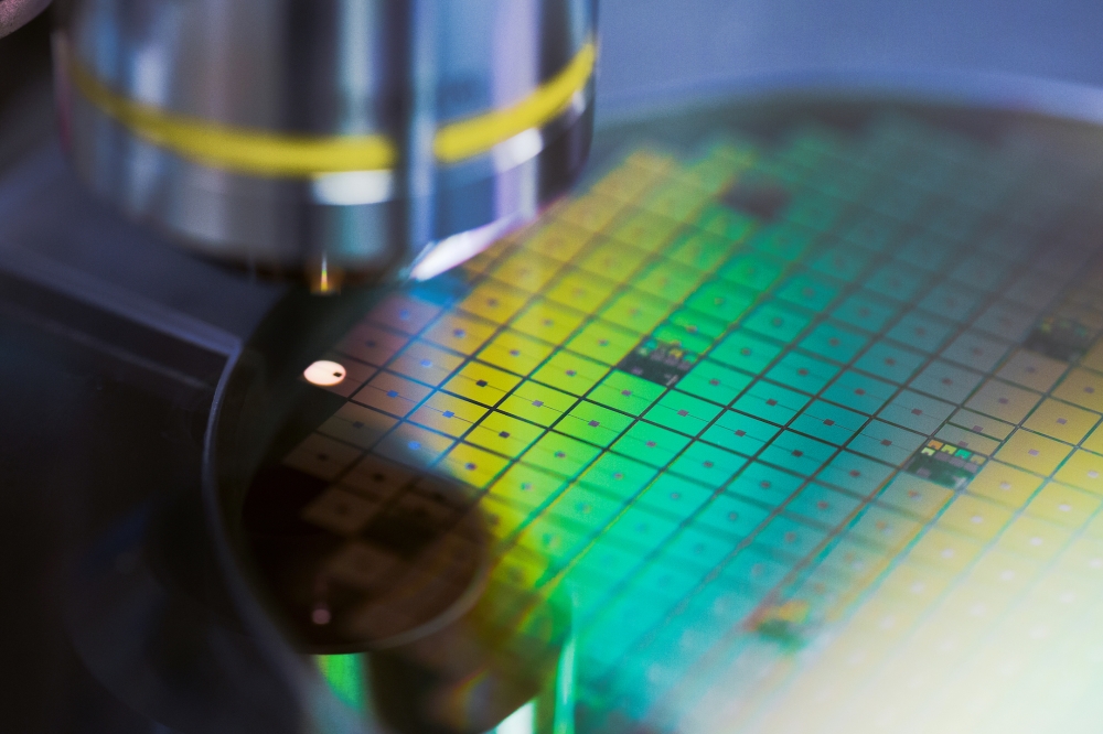
Electrical Testing in Nexperia’s R&D Labs
… and SiC power portfolios
In the last year or so Nexperia has expanded its SiC portfolio, to include 650 V diodes with current rating from 6 A to 20 A, in a range of formats that incorporate both surface mount and through-hole configurations.
Additional advances are the launch of the first automotive-grade product, announced at this year’s PCIM conference, and first design wins, especially in power supply applications.
Feurle describes the relationship with Mitsubishi Electric, which is key to the production of discrete SiC MOSFETs, as a strategic collaboration that’s mutually beneficial for both sides. She says: “It’s supporting the mission of Nexperia, but also Mitsubishi, to meet the rapidly growing demand for silicon carbide.” By combining complementary expertise, both partners are reducing requirements for in-house development, and enabling them to go faster to market.
Obstructing Nexperia’s plans has been its forced sale of its fab in Newport, Wales, a move dictated by the UK government. While this has caused serious disruption, it has not impacted Nexperia’s compound semiconductor activities, as there were no plans to reintroduce them at the Newport site.
At the Hamburg fab, conversion of office space to clean rooms is underway, and the first new tools have arrived. Over the next few years, engineers will establish lines for SiC and GaN production, with full production slated for 2027.
“Selected key customers, of course, will receive samples in advance, to be able to qualify dedicated target applications,” remarks Feurle.
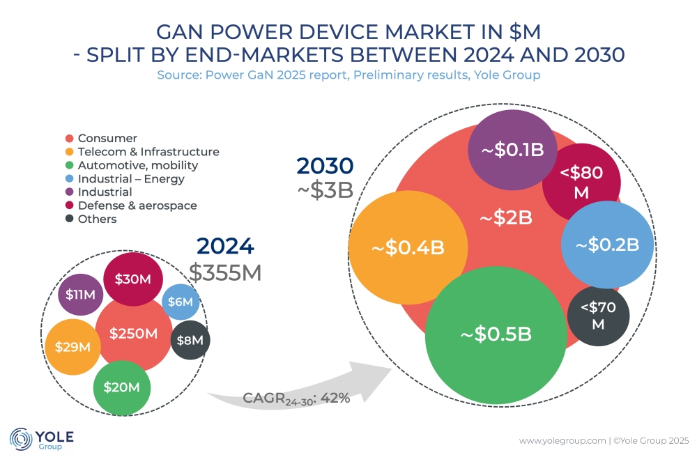
The balance between the production of SiC and GaN devices will be determined by the market. Today SiC dominates, but the gap is expected to narrow, with Castro expecting that by 2028, the SiC market will be around four times that of GaN.
Based on this forecast, and Nexperia’s substantial investment, this chipmaker is sure to be a significant supplier of a wide range of wide bandgap devices by the end of this decade.