Power GaN: The 300 mm milestone
Migrating the manufacture of GaN power devices to 300 mm lines will boost yield, improve metrology and trim costs.
BY RICHARD STEVENSON, EDITOR, CS MAGAZINE
A common metric for measuring performance of any device is the bang per buck.
When it comes to GaN, there are many ways to measure that ‘bang’. They include the on-resistance, the breakdown voltage, and the mobility of the two-dimensional electron gas.
But what about the ‘buck’? That’s a little harder to fathom, as chipmakers rarely reveal their yield, or the cost of producing their devices. But there are occasions when they will champion their efforts to trim their manufacturing costs, such as a move to larger wafers.
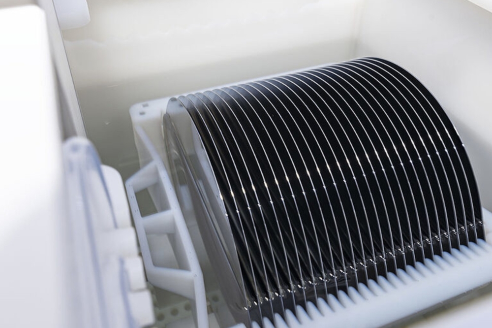
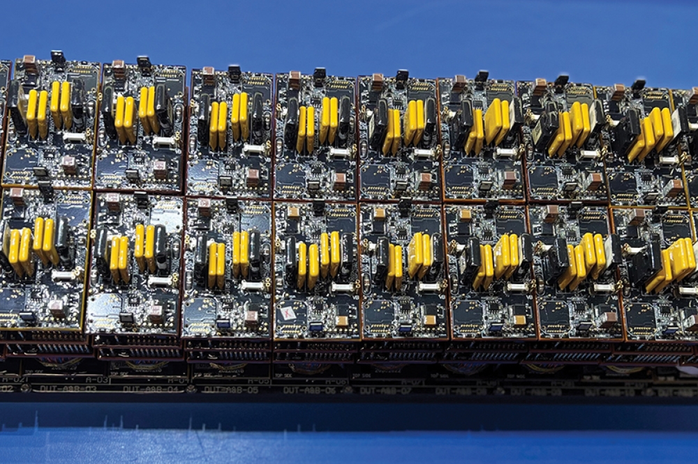
Claiming significant success on this front is the well-known European producer of power electronics, Infineon. It grabbed the headlines this autumn, when announcing the fabrication of the first GaN power devices on 300 mm wafers.
With manufacturers of GaN-on-silicon HEMTs currently carrying out production on substrates with a diameter of 200 mm, and sometimes less than that, Infineon’s milestone is more than doubling the number of devices produced per wafer.
Note, though, that this gain is not the only one that will help to trim the cost of production. According to Johannes Schoiswohl, Infineon’s Business Line Head for GaN, migration to larger wafers also leads to improvements to the manufacturing process, such as a higher yield and access to superior metrology. Engineers at Infineon enjoyed these when progressing from 150 mm to 200 mm wafers, and they are seeing them again in the move to the 300 mm platform.
“We can get really great results – better than expected – because the 300-millimetre tools, from a performance perspective, from a monitoring perspective and a process control perspective, are better than the 8-inch tools,” remarks Schoiswohl.
Due to these benefits, Infineon took just 18 months to develop its 300 mm process, building on its 200 mm GaN-on-silicon technology.

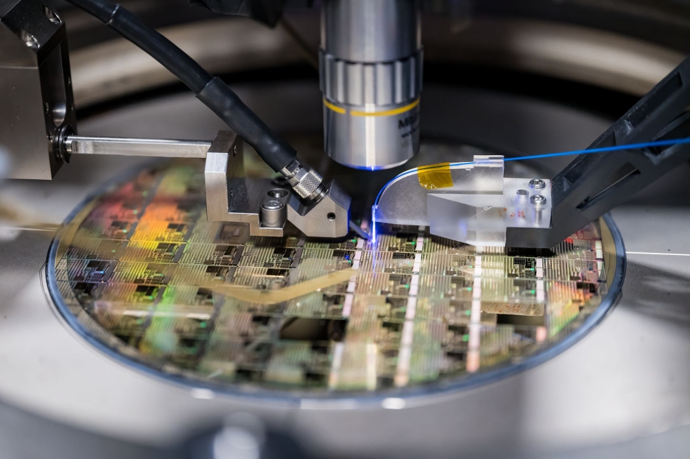
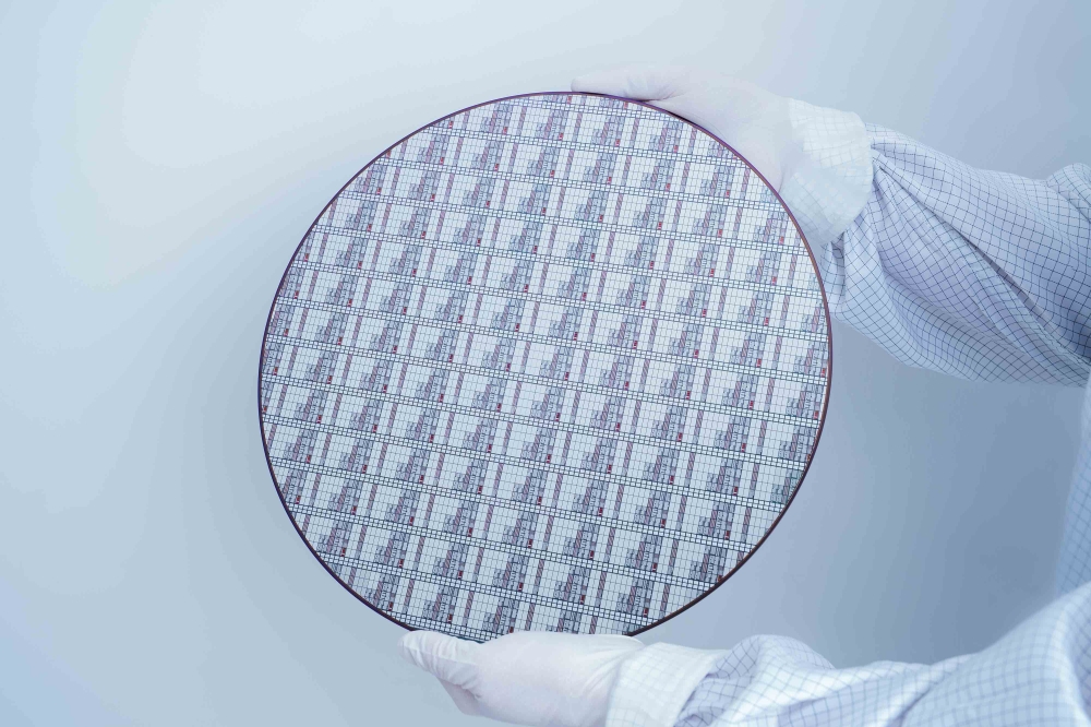
A technical engineer in the cleanroom at Infineon Technologies in Villach, Austria, holds a 300 mm GaN-on-silicon wafer.
According to the company’s projections, its GaN power devices could reach cost parity with their silicon equivalents. Helping to reach this goal will be: economies-of-scale; improvements in the technology itself, particularly the epitaxial stack; and the lower on-resistance of GaN, enabling smaller die to deliver the same performance as comparable products made from silicon.
To develop its trailblazing technology, Infineon’s engineers have had to grapple with the lattice mismatch between GaN and silicon, as well as differences in thermal expansion coefficients.
“The bigger the wafer diameter, the harder it gets,” admits Schoiswohl. “The wafers start to bow because of the lattice mismatch, and at a certain epi-thickness, they simply crack.”
By developing and refining its epitaxial technology, Infineon releases strain during the growth.
Schoiswohl says that the particular epitaxial processes employed by providers of GaN power transistors are a key differentiator. According to him, the quality of the epitaxy determines the degree of early lifetime failures and often defines the device’s failure mechanisms.
With Infineon’s GaN power devices, a thicker epitaxial stack is needed to realise a higher blocking voltage. According to Schoiswohl, the company’s engineers can see a path to progressing from 100 V to 650 V devices, but going beyond that will be more challenging. He says that one solution could be a switch to thicker wafers: “These are all details we have to figure out.”
Infineon already offers wide bandgap power devices operating at a kilovolt or more, based on SiC. But that will not stop the company investigating what might be possible with GaN, which offers the tantalising possibility of a better performance at a lower cost.
Following the production of GaN-on-silicon epiwafers on dedicated MOCVD tools, processing of this material is undertaken on standard silicon lines – that’s a significant merit from a CapEx perspective.
Infineon’s pioneering work has been carried out at its facility in Villach, with attention paid to ensuring that processing of its GaN-on-silicon wafer in a 300 mm line did not introduce any contamination. As volume ramps, there will come a time when a 300 mm line can be devoted solely to the production of GaN devices. Infineon also has 300 mm equipment in Dresden that could be used for the production of GaN devices, and opportunities to potentially outsource due to established foundries.
At the upcoming trade show Electronica, to be held in Munich from 12-15 November, Infineon will release its next-generation G5 HV technology. The plan is to take this process and apply it to 300 mm wafers, with engineering samples reaching customers by the end of next year, and production ramping in 2026.
Today the biggest market for GaN power devices is consumer chargers. “We can see that this is now reaching points where some customers say 100 percent of their volume will move there,” remarks Schoiswohl.
Additional opportunities are found in power supplies for AI, motor controls and inverters, as well as the automotive industry. While all these markets are important, Schoiswohl sees the automotive sector as an important one, due to the opportunity for higher volumes, with GaN a compelling candidate for the on-board charger.
Success will hinge on the bang-per-buck, helped by a move to 300 mm GaN-on-silicon.