Clas-SiC expands technology in its stride
Not content with opening the world’s first SiC foundry that partners
with power device designers, Clas-SiC Wafer Fab is evolving and adapting
to grow its success.
BY JEN WALLS AND DAVID CLARK FROM CLAS-SIC
Founded in 2017, Clas-SiC Wafer Fab is the world’s first open foundry dedicated to SiC. At our facility, located in Lochgelly on the outskirts of Scotland’s capital city, Edinburgh, we have adopted a pure-play approach, which means that we’ll never be in competition with our device customers. Instead, they draw on our standard process flows and flexible Process Design Kits (PDKs) to simply and quickly design highly customised SiC devices. By using PDK models to minimise non-recurring engineering and trim the cost and cycle time, our customers can work with us to produce a range of competitively priced SiC transistors and diodes operating at 650 V, 1.2 kV, 1.7 kV and 3.3 kV on both conventional and engineered SiC substrates.
Our mission is to provide a low barrier to entry for all of our customers seeking to develop new products. We support them at every step, from proof-of-concept to market seeding, low-volume production, right through to high-volume production. This sets us apart, as we are the only foundry in the SiC industry that takes customers through all stages of product lifecycle. Most of our business comes from the manufacture of enhancement-mode MOSFETs, but we also produce depletion mode MOSFETs and two forms of diode – the merged p-i-n Schottky diode, and the junction barrier Schottky diode. We use PDKs to support a high level of integration, during successful customer designs for highly customised unique devices, even to the extent of including integrated sensors as part of the device design. Our customers can have confidence in these PDKs – as well as having reliability proven on our reference devices, they have been used by customers that conduct reliability trials on their own specific devices, with efforts on this front demonstrating that our foundry produces devices that satisfy AEC-Q101 using JEDEC 22 conditions.
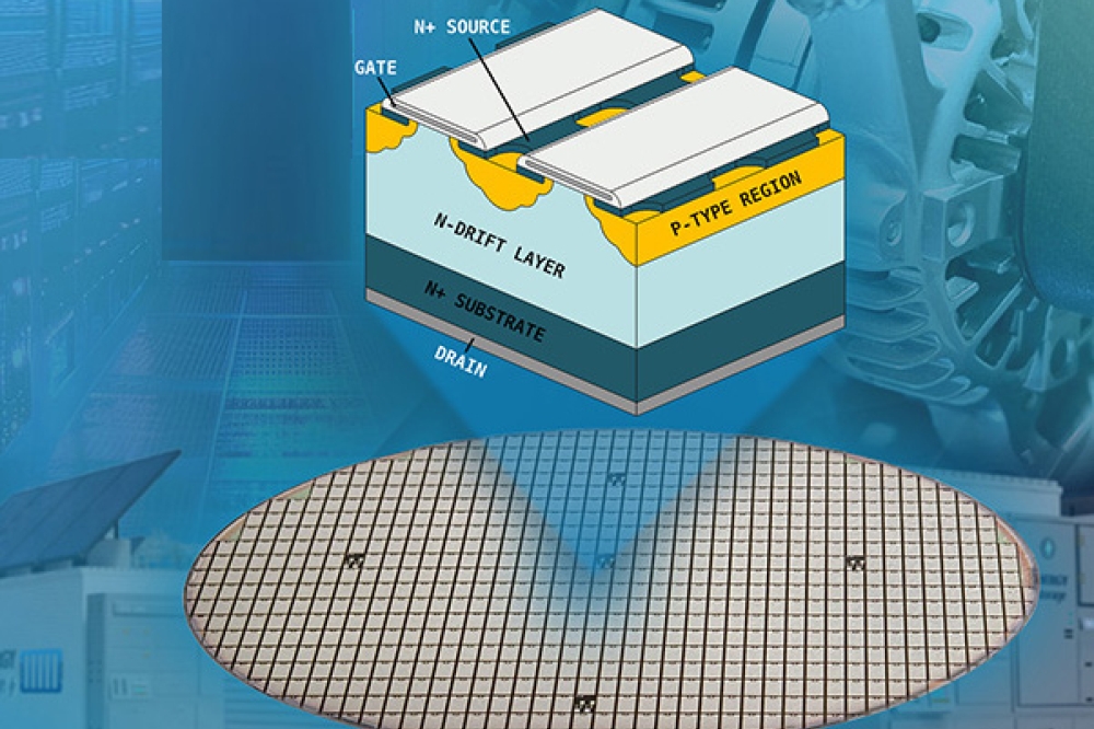
Since releasing our initial generation of PDKs in 2022, we have been working on developing Generation 3 PDKs. These successors deliver significant improvements in the performance of 1.2 kV planar MOSFETs, realised by shrinking transistor dimensions (see Figure 1). With favourable wafer-level results, Generation 3 devices are currently undergoing reliability trials, ahead of a scheduled release at the end of 2024. In parallel we are qualifying devices fabricated on engineered substrates to add to our PDK offerings.
Figure 1. Reducing the width of the JFET is leading to a reduction in specific on-resistance.
We are now starting to turn our focus to Generation 4 MOSFETs. They feature a shrinking of the transistor interconnect, a refinement that enables a further reduction in cell pitch and thus a corresponding reduction in specific on-resistance. To produce these transistors, we are investing in upgrading and expanding our tooling.
Right now, we are on the cusp of this exciting new phase, with the new tooling being identified, procured and installed ahead of interconnect technology development. Our timescales are governed by tool delivery times, and we are forecasting the introduction of our Generation 4 PDK in 2026. We plan to begin our Generation 3 and 4 technologies on 1.2 kV MOSFETs, before subsequently extending this technology to 1.7 kV and then 3.3 kV variants.
While we are currently focusing on planar MOSFET technology, this has not stopped us from conducting trench processing work for specific customer projects. As part of this effort, we are investing in process tooling to expand our trench processing capabilities, and support the possibility of developing our own trench MOSFET PDKs in the future.
We have drawn on our standard process modules that underpin our PDKs to fabricate novel trench and planar SiC MOSFETs, using heavily customised process flows. In addition, we have adopted this approach to produce p-n diodes, JFETs, and other customised devices, including both lateral and vertical device architectures.
As well as producing a wide range of SiC devices, we are active in UK innovation-based funding calls. They include APC (Advanced Propulsion Centre), DER (Driving the Electric Revolution), as well as the EU Horizon scheme. Projects in progress include an automotive BEV/FCEV project, a Solid-State Transformer project, and a project for Condition & Health Monitoring in Power Electronics. To keep close to technology advances, we are maintaining close academic links with research teams in the UK, at the University of Glasgow and Warwick, as well as overseas, such as at Purdue University.
Our innovation surrounding process development extends beyond ‘normal’ process advancements. We are closely involved in wafer fabrication tool development, partnering with major industrial players that advance semiconductor equipment design. This extends through to our work with substrate and epitaxy providers, to help them validate their materials for the market. Through this work we are advancing the world of SiC device processing.
As well as technology development, which is the R&D part of our business and where we tend to begin our engagement with customers, we have another two business streams. They are Low-Rate Production (LRP), and Licensing, Royalty and Consulting (LR&C) (see Figure 2 for a summary of our business streams).
Figure 2.The business stratergy of Clas-SiC Wafer Fab
Our LR&C business stream enables customers with ambitious expansion plans to ramp up to high-volume/low-cost manufacture. This initiative provides support for independent foundries in low-cost manufacturing locations, such as those in Asia, to set up replicas of Clas-SiC processes. Our capacity in Scotland is limited to low-rate production, so this model allows us to access much higher volumes without Capex investment, keeping prices down for our customers.
For those that work with us under LR&C contracts, the norm is that a defined portion of their capacity is reserved for Clas-SiC customers. When our customers outgrow the capacity of Clas-SiC foundry, we outsource production to one of these associated but independent fabs. Throughout this evolution our customers maintains their partnership with us, utilising our advancing PDKs for their next-generation devices as they start another R&D cycle.
The first wafer fab utilising this model is now well advanced. Supported by our team, this fab has been constructed, facilities and tooling are installed, processes have been set up, and production will soon begin. We also have a number of other potential LR&C projects at the stage of advanced discussion.
Key to our success is our continual re-investment, not only in capital equipment, but also in our people. Our staff, with their advanced skill sets and out-of-the-box thinking, are our greatest asset. We now have more than 320 man-years of experience in SiC device processing, putting us in an unrivalled position for taking on the challenges of our customers. We pride ourselves in the continual development of our workforce, from our production operators through to our senior management team.
Training has been crucial to our advancing over the last year, as we have undergone exceptional growth and transitioned to a 24/7 operation for device production. More than 80 percent of our direct labour has received advanced training to fully utilise and build their skillsets, a move that has led to a more flexible and satisfied workforce. Our investment in new entrants, in the form of modern apprentices and graduate apprentices, is also well advanced. As well as ensuring that we keep the talent pipeline in a healthy state, this introduction of ‘young blood’ maintains a well-balanced age demographic within our workforce.
Despite the tough investment environment throughout the world, we have managed to secure equity investment from Archean Chemical Industries Ltd. We are excited to have them on our team and looking forward to the exciting times ahead. This funding will help to grow our business, supporting the launch of Gen 4.0 technology in 2026, as well as strengthening our Board of Directors.
We have been privileged to have both the financial support and the wisdom of knowledgeable investors since our foundation. One of our founding members, Carl Johnson, launched a CdTe crystal growth company just over fifty years ago that has blossomed into Coherent. By drawing on this expertise, we are well supported in our efforts that will see us take Clas-SiC to the next level and beyond.

