Boosting AlN-on-AlN Schottky barrier diode performance
Engineers at Arizona State University are claiming to have delivered a significant breakthrough in the performance of AlN Schottky barrier diodes.
“Our work is the first demonstration that simultaneously achieves an ultra-low ideality factor and a high breakdown voltage for AlN diodes,” remarks team spokesman Houqiang Fu.
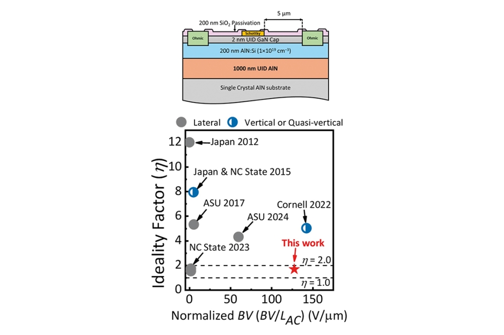
One of these metrics, the ideality factor, is used to evaluate the quality of a diode, with better devices having lower values. For diodes made from many materials, ideality factors typically range from 1 to 2, but for those made from AlN much higher values have been reported, due to defect-induced current transport mechanisms in the AlN epilayers. Researchers have recorded values for AlN Schottky barrier diodes that range from 5 to 12.
“[Our] work presents an ultra-low ideality factor of 1.65, combined with a high breakdown voltage of 640 volt,” says Fu, adding that while an even lower value of 1.5 has been reported by another group, that’s for a device with a much lower breakdown voltage.
Fu says that realising AlN Schottky barrier diodes with ideality factors close to one is challenging, due to the relatively low maturity of AlN epilayer growth and subsequent fabrication processes, and the difficulty in forming good ohmic and Schottky contacts.
The team’s success comes from addressing all these issues. “Growth of AlN epilayers on AlN substrates is crucial for developing high-quality layers with low defect and dislocation densities,” argues Fu, who adds: “The device design, particularly the anode-to-cathode distance, is critical for optimising thermionic emission current.”
Device fabrication began by loading AlN substrates with a dislocation density of around 103 cm-2 in an MOCVD reactor and depositing, at 1250 °C, a 1 mm-thick AlN buffer, followed by a 200 nm-thick AlN layer that’s heavily doped with silicon and an unintentionally doped 2 nm-thick caping layer.
According to atomic force microscopy and high-resolution X-ray diffraction measurements, the epiwafer has a smooth surface morphology, with a root-mean-square roughness of just 0.4 nm, and a full-width at half-maximum of just 17 arcseconds for the (0002) rocking curve.
Based on the latter result, the team claims that switching the substrate from sapphire to single-crystal AlN slashes the defect density in the epilayers by over three orders of magnitude.
Schottky barrier diodes were fabricated using conventional optical lithography and lift-off processes, with circular ohmic contacts with a
100 mm diameter formed from a Ti/Al/Ni/Au stack, and Schottky contacts of the same size produced by electron-beam evaporation of a Ni/Au stack. These diodes, with a cathode-to-anode distance of 5 mm, were passivated by plasma-enhanced CVD of a 200 nm-thick layer of SiO2, and had contact vias opened by reactive ion etching.
Electrical measurements on these diodes revealed that increasing their temperature from ambient to 573K produces a fall in ideality factor from 1.65 to 1.23, an increase in Schottky barrier height from 1.94 eV to 2.41 eV, and a hike in on-off ratio from 107 to 109.
Destructive breakdown of these diodes at 640 V is primarily caused by crowding of the electric field under the anode edge.
Fu reveals that the next step will be the development of AlN Schottky barrier diodes with near-unity ideality factors and multi-kilovolt breakdown voltages, realised through the introduction of field plates and effective passivation techniques.
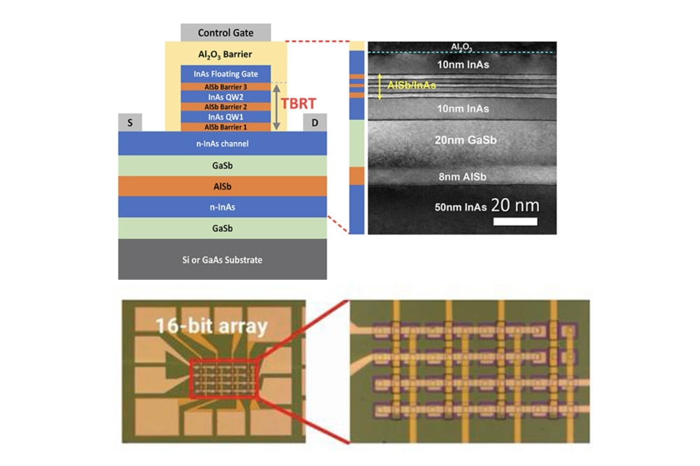
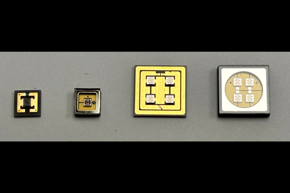
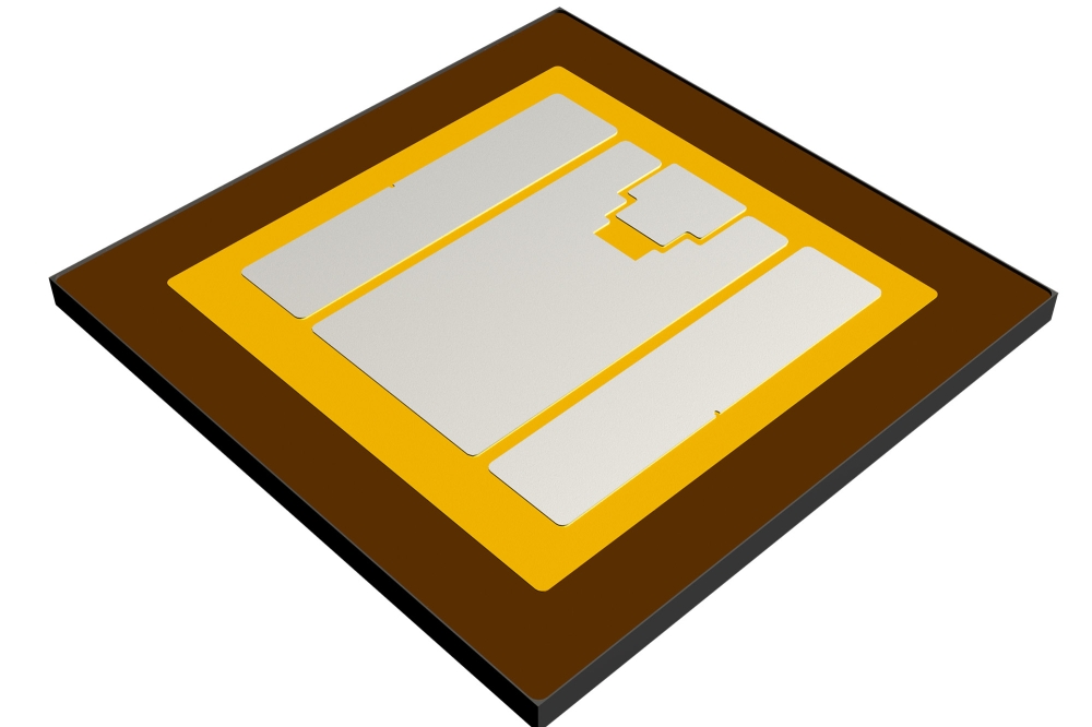
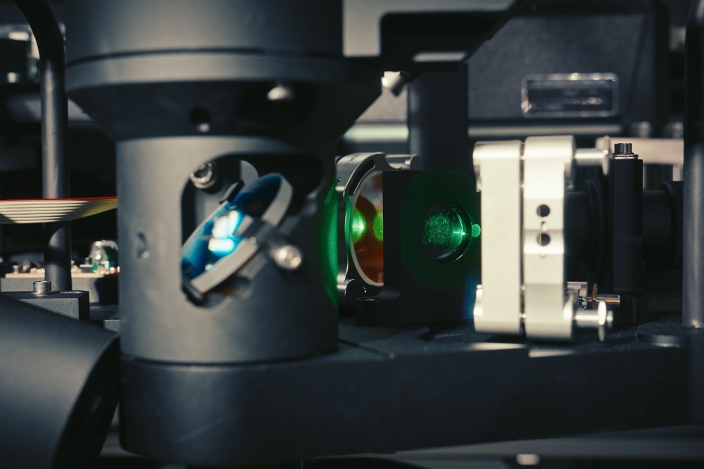
Pictured above: AlN Schottky barrier diodes fabricated at Arizona State University break new ground in terms of the combination of blocking voltage and ideality factor.
Reference
D. H. Mudiyanselage et al. Appl. Phys. Express 17 074001 (2024)

