Scrutinising traps in GaN MOS-HEMTs
Experiments expose the physical and energetic locations of defects that are impairing the performance and reliability of GaN MOS-HEMTs operating in 5G millimetre-wave bands
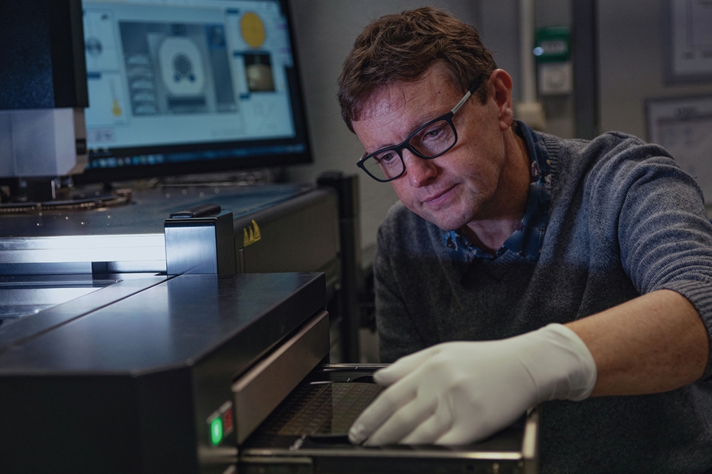
BY BARRY O’SULLIVAN FROM IMEC
Today’s mobile technology bears little resemblance to that of the 1980s. Long gone are the days when the only capabilities of the handsets were to make calls and send texts limited to 160 characters. Now mobiles combine the capabilities of a computer with an impressive camera for stills and video, and provide great communication almost everywhere, a benefit that is realised by uploading and downloading a tremendous amount of data at high speeds.
The latest generations of smartphones, and how they are used, account for the explosive growth in data traffic and an unabating need for higher bandwidth. Both show no signs of slowing, and are more likely to accelerate, due to the onset of a new era that will incorporate artificial intelligence and virtual reality.
Helping to support the eye-watering ramp in data traffic is the steady upgrade to wireless infrastructure. Now being rolled out in its fifth-generation format, known simply as 5G, the latest technology is offering a significant leap in capabilities. When operating today at sub-6 GHz frequencies, 5G combines unprecedented data rates with ultra-low latency and the capacity to connect a massive number of devices simultaneously. This wonderful set of attributes is paving the way for a number of new applications, including smart cities, autonomous vehicles, and the Internet of Things (IoT).

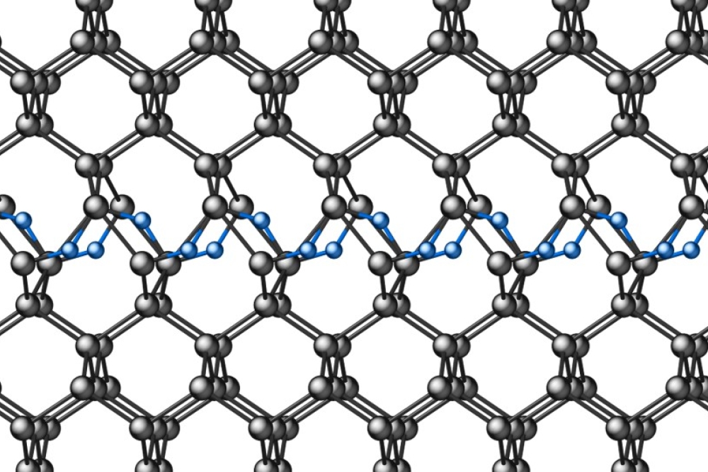
Figure 1. A design of MOS-HEMT devices with a gate dielectric deposited in a partially recessed AlGaN layer.
The sub-6 GHz devices that are currently available are based on silicon-on-insulator technologies that utilise the scalability of the silicon microelectronics industry. However, this particular material system is held back by fundamental limitations in speed, an impediment that’s opening the door to compound semiconductor materials, which have the potential to supplant silicon-based devices as the primary foundation for next-generation RF technologies.
This promising family of alternatives includes SiGe, InP and GaN. The latter is the stand out candidate, due to its superior electron mobility, high breakdown voltage, and its capacity to operate at higher frequencies and powers. Drawing on these strengths, allied to excellent thermal stability and efficiency, ensures that GaN-based devices are ideal for RF and microwave applications, including 5G infrastructure, radar, and satellite communications.
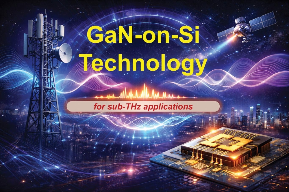
GaN-on-silicon technologies
At imec, we are currently investigating the potential of GaN-on-silicon technologies for millimetre-wave RF applications in the FR3 frequency range, which spans around 7 GHz through to 25 GHz. Our decision to work with GaN power amplifiers stems from their superior output power over other technologies at millimetre-wave frequencies, and when fabricated on silicon, their cost benefits. For this class of power amplifier, the core transistors are AlGaN/GaN HEMTs – they are renowned for their high-frequency performance and their ability to handle high power.
Scaling is a crucial lever for optimising the performance of RF transistors in applications for 5G and beyond. This miniaturisation can be lateral, involving a trimming of the width and length of the transistor, or vertical, realised by reducing the thickness of the layers. Benefits of lateral scaling include enhancing the speed and frequency response, while concomitant vertical scaling is required to tackle short-channel effects that threaten to degrade transistor performance. However, continued vertical scaling is a concern, as it can lead to an increase in leakage currents, particularly when the transistor is in the on-state.
One option for combating a scaling-induced hike in leakage current is to insert a high-κ dielectric between the gate metal and the AlGaN barrier. It’s a move that creates a metal-oxide-semiconductor HEMT (MOS-HEMT) structure.
High-κ dielectrics are well-stablished, having been used in silicon technologies for the same purpose – to reduce leakage in ultra-scaled transistors – for the last 20 years. But their widespread application does not guarantee success, as they are notoriously defective materials. Due to reliability challenges faced when incorporating them in silicon-based logic devices, it is critical to study the impact that they have in MOS-HEMTs.
Here we present the key findings of one of the first reliability studies for GaN-on-silicon MOS-HEMTs for power amplifiers, an investigation that we first reported at the 2024 IEEE International Reliability Physics Symposium (IRPS) and published in its proceedings.
An important finding from our study is that there is charge trapping and emission in the HEMT-structures with high-k dielectrics. During our investigations, we successfully isolated the physical and energetic location of the responsible defects. We found that trapping and emission occur when charge carriers in the device are confined in, or released from, certain defects in the semiconductor or dielectric material. These processes impact the performance and the reliability of the HEMT, especially in high-frequency and high-power applications. Another outcome of our research is that it has identified the best material combinations and layer thicknesses for overall device process optimisation.

Figure 2. The charge trapping characteristics of MOS-HEMT structures with HfO2 or Al2O3 high-k layers. Al2O3 results shows the threshold voltage, Vt, increasing as function of time and bias, suggesting defect types with a wide energy range. HfO2, on the other hand, shows negligible trapping at low biases but, there are significant Vt shifts at higher bias. This points to a relatively narrow defect type in this bias range. Figure based on O’Sullivan et al. IRPS 2024.
Capturing electrons from the dielectric
A primary reliability concern affecting the MOS-HEMT is bias temperature instability (BTI), an affliction that leads to device degradation over time, due to prolonged exposure to electrical stress (bias) at elevated temperatures. The root cause of this issue is a trapping of electrons, either in the dielectric or at the interface between the dielectric and the semiconductor layers. One consequence of BTI is a gradual shift in threshold voltage. Due to this shift, transistors require more voltage to switch on, and ultimately circuits are slower and less efficient.
We have mimicked BTI by applying a DC voltage or ‘stress’ to MOS-HEMTs with HfO2 and Al2O3 high-κ dielectrics and monitoring the shift in threshold voltage. For variants with Al2O3-stacks, the threshold voltage increases with time and bias, indicative of defects present over a wide bias and energy range. In the case of HfO2, we observe two modes of degradation. At lower voltages the plots show HEMT-like time-independent and negligible charge trapping, while at higher stress bias we see significant threshold voltage shifts, with a power law increase with time and bias until saturation at around 300 mV. This high degree of bias dependence suggests a relatively narrow defect type in this stress range.
A key question is this: Are charges trapped in the bulk dielectric or at the interface? We are able to differentiate between these two locations by observing how the shift in threshold voltage responds to changes in thickness of the high-k dielectric, using capacitance measurements and simulations. This approach has determined that most of charge trapping happens in the bulk dielectric.

Figure 3. (Top) Emission kinetics of (left) HfO2 and (right) Al2O3 MOS-HEMTs after stressing for increasing times. Note the difference in emission behaviour between Al2O3 and HfO2, which only partially emits. (Bottom) Fitting data to the universal relaxation model shows that HfO2
emission is described by (left) a recoverable component, (right) a
permanent component and a third component, as the data doesn’t match the
fit well. Figure based on O’Sullivan et al. IRPS 2024.
Emission behaviour: 3 types of defect?
Switching off the stress that’s applied to MOS-HEMTs can lead to the release or emission of trapped charges. By analysing these emission dynamics, it’s possible to gain insight into the reliability of the device, by looking at the recovery of the threshold voltage, and the origin of the defects.
Our results reveal that the defects responsible for the shift in threshold voltage in Al₂O₃ MOS-HEMTs release their charges quickly and completely. In comparison, devices with HfO₂ emit charges more slowly, and this process remains incomplete. Based on these findings, there is a difference in the nature of the defects responsible for charge trapping on changing the dielectric material.
To determine how many types of defects are present in our HfO2 MOS-HEMTs, we fitted our experimental results to the universal relaxation model. This model assumes that for every type of defect present, the individual defects of that nature have their own characteristic energy, following a certain distribution.
Fitting this model to our HfO2 data clearly shows that more than one defect level is at play; the emission data is not overlapping the model. Our simulation only considered defects that display complete emission, a situation that occurs when the threshold voltage is recovered. However, in some cases the trapped charges do not emit from the defect, and the change in threshold voltage is permanent. When this permanent component is added to the model, it aligns more closely to the experimental data. Note, though, that the fit is not perfect. While the difference might only be 10 mV, this suggests that there are a total of three different defect types present in the HfO2 MOS-HEMTs.
This finding differs from previous studies on Al₂O₃ dielectrics. According to these reports published in the literature, only two defect types contribute to the charge trapping in Al₂O₃ dielectrics. However, there is a wide distribution of defects in Al₂O₃ that complicates further detailed analysis.

Figure 4. (Left) The activation energy map for HfO2 MOS-HEMT showing the three defect types modelled to explain the measured BTI behaviour. (Right) Simulated band diagram of HfO2
MOS-HEMT, showing electrons filling the shallow defect during capture
and emission from 3 defect types. Emission from the shallow defect can
be either to the channel (recoverable) or the AlGaN conduction band
(non-recoverable), while simultaneously the deep HfO2 level can be charged, explaining the increasing threshold voltage, Vt, seen at low temperatures. Figure based on O’Sullivan et al. IRPS 2024.
Scrutinising HfO2 devices
The next step in our study involved investigating how the defects in HfO2 MOS-HEMTs contribute to the threshold voltage shift. Armed with this knowledge, we gained greater insight into device stability.
By calculating the activation energy that’s needed for defects to capture and release charges, we have mapped out three different defect types for HfO₂. They are: a low thermally-activated defect, which we name as R1, that captures and emits electrons quickly; and a pair of higher activation-energy defects, denoted R2 and R3, that have similar charge capture rates but emit charges differently.
According to the band diagram for our HfO2 MOS-HEMTs, during application of the bias voltage, electrons are captured into a shallow defect in the dielectric, located about 2 eV below the conduction band of HfO₂. As this defect level is not accessible energetically at a low stress bias, charge trapping becomes more pronounced at higher voltages.
The band diagram also helps explain why the removal of the bias causes some of the captured electrons to be emitted back into the GaN channel, leading to a recoverable threshold voltage shift (R2). That’s not the case for all electrons, with some still trapped in the energy barrier between the HfO₂ and AlGaN layers, a situation that results in a permanent threshold voltage shift (R3). This difference in emission behaviour reveals that while the same defect type is behind the threshold voltage shift, it must be modelled as two separate defects, due to the two emission pathways.
We have also identified a deeper defect, about 3 eV below the conduction band, that contributes to the negative threshold voltage shift (R1). These electrons are trapped during the recovery phase.
Improving reliability
This study of ours provides crucial insights into how different high-κ dielectric materials, particularly HfO2 and Al2O3, affect the performance and reliability of MOS-HEMT devices. By identifying multiple defect types in HfO2, with varying charge capture and emission characteristics, we highlighted how these materials respond differently under electrical stress.
Based on our findings, we would argue that Al2O3, with its faster charge recovery, probably offers better stability for applications requiring rapid switching. Meanwhile, HfO2 shows more persistent threshold voltage shifts due to slower emission, which could impact long-term device reliability. Additionally, HfO2 has higher defect densities, but they are energetically distributed across narrow energy ranges, whereas Al2O3 has a lower density of defects, but the responsible defects are distributed over a broader energy range. These insights are invaluable for optimising material combinations and layer thickness choices in high-frequency, high-power devices, allowing for improved designs that balance performance and durability across a range of applications.
Our next step is to compare our results with those for enhancement-mode HEMTs, which are devices that have a threshold voltage that’s greater than 0 V. Intrinsically, HEMT-structures are depletion-mode devices – that is, the device is switched on at 0 V – but enhancement-mode operation is preferred for RF applications, as it reduces power consumption and increases reliability. Another benefit of enhancement-mode operation is that it simplifies circuit design, eliminating the need for either: voltage shifters, which create the negative voltage to switch off depletion-mode transistors; or for a multi-step device turn-on, which prevents short-circuits and power surges in depletion-mode devices.
Looking further ahead, we plan to study the RF performance of MOS-HEMTs with these dielectric layers, as well as the interaction between defect levels.