Revolutionising semiconductor etching
Metal-assisted chemical etching is a damage-free process that produces trenches with an unprecedented aspect ratio.
BY XIULING LI FROM THE UNIVERSITY OF TEXAS AT AUSTIN
In the rapidly advancing world of semiconductor technology there’s a relentless drive to scale device dimensions. Motivating this miniaturisation is a combination of enhancing performance, reducing power consumption, and increasing density across a wide range of applications – from logic and memory, to RF, photonics, and sensing. However, shrinking feature sizes and moving integration in the third dimension creates significant challenges for traditional etching techniques, which struggle to realise ultra-high aspect ratio vertical structures while preserving material integrity.
Offering much promise in this regard is metal-assisted chemical etching. This groundbreaking technique, also referred to as MacEtch or MACE, provides ultra-high anisotropy etching that’s free from damage. It is an innovative approach that effectively addresses the limitations of conventional methods, and enables aggressive scaling of semiconductor devices and integration.
Here we explore the principles, applications, and future prospects of MacEtch. It’s a technique that we are advancing at the University of Texas at Austin that has the potential to reshape the landscape of semiconductor manufacturing.

Figure 1. Illustration (not to scale) of the effect of
sidewall damage (assuming 1 µm depth) with microLED device size scaling – the
damage does not scale and hence the percentage of luminous area reduces
significantly with size.
Detrimental damage
One of the most widely used techniques in semiconductor
manufacturing, inductively coupled plasma reactive ion etching (ICP-RIE),
offers high etching rates and excellent control over anisotropy. However, the
presence of high-energy ions in the plasma tends to result in surface and
sidewall damage, which becomes increasingly detrimental at reduced feature
sizes. The damage manifests as lattice defects, such as vacancies,
interstitials, dangling bonds, surface roughness, and impurity accumulation.
An unwanted consequence of this damage is that it drags down device performance. Electronic devices may suffer from increased leakage currents, reduced speed, and lower breakdown voltages, issues that stem from the introduction of traps and degraded mobility; while optoelectronic devices can be impaired by a reduced efficiency, due to surface scattering and non-radiative recombination.
An example of the downside of RIE is that when it’s used to process LEDs, device efficiency falls, primarily due to sidewall damage during etching. It’s an issue that’s particularly acute in microLEDs – as damage does not scale, the proportion of luminous area reduces significantly with device size (see Figure 1). Due to this damage, the external quantum efficiency of a blue-emitting microLED with dimensions of 5–10 μm is usually no more than 20 percent, a figure that falls far short of 70 percent, which can be realised with a broad-area blue LED.

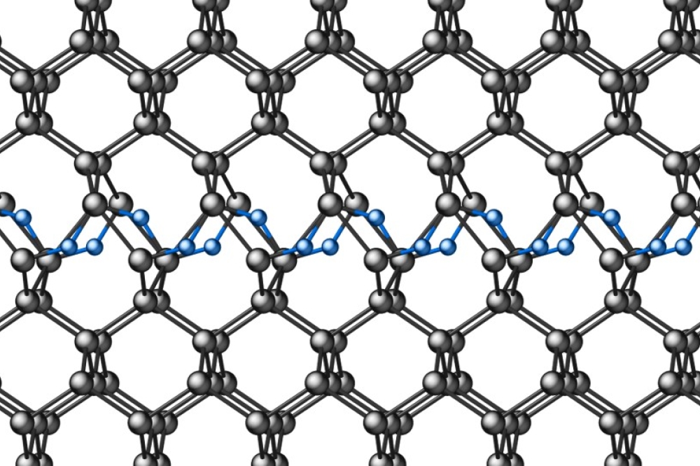
Figure 2. MacEtch process illustration and a scanning
electron microscopy image of an array of silicon nanowires (diameter = 550 nm,
depth = 51 μm) produced by gold-MacEtch. For more details, see X. Li., Curr. Opin. Solid State Materi. Sci.
16 71 (2012) and K. Balasundaram et al. Nanotech. 23 305304 (2012).
When working with silicon, etch damage can mostly be
repaired by thermal annealing if the thermal budget allows. But that’s not the
case for compound semiconductors – they are limited by different requirements
for each element in the compound to restore lattice crystallinity and
stoichiometry; the damage is extremely difficult to repair completely; and, in
some cases, damage is irreversible. These problems are exacerbated when device
or circuit dimensions or densities are of the order of tens of nanometres, a
length scale where surface damage is detrimental. Due to these concerns, it is
paramount to find a solution that allows precise, damage-free etching, a
crucial requirement for continued scaling of semiconductor technologies.
The conventional strategies for mitigating the damage caused by traditional ICP-RIE involve process optimisation. It’s a task that demands the careful tuning of etching parameters, such as RF power, pressure, and gas flows, while maintaining etch rates and anisotropy; and it also requires the application of post-etch treatments, such as annealing or wet chemical treatments. However, these approaches often compromise the etch rate, anisotropy, or feature density, making ICP-RIE less suitable for high-throughput manufacturing. What’s needed is a fundamentally different approach that is not held back by these limitations.
Not your ordinary etching
Defying the isotropic nature of the conventional chemical
etch, MacEtch is an open-circuit, anisotropic etching method that is
plasma-free, causes no damage and can take place at near-room temperature.
Thanks to these strengths, MacEtch promises to transform the production of
three-dimensional device structures for various electronics, photonics, energy,
quantum, and sensing applications, and three-dimensional heterogeneous
integration.
MacEtch relies on a local catalysis and an electron-transfer effect to enable site-controlled semiconductor nanostructure fabrication (see Figure 2 for a silicon MacEtch example). For this form of etching, a metal-patterned semiconductor is immersed in an acid (or base) and an oxidant mixture; and a metal catalyst is employed to provide anisotropic selectivity, by lowering the activation potential of the etching reaction locally. During this process, the semiconductor functions as the anode and the metal serves as the cathode. A local electrochemical cell under open circuit is created by the metal/semiconductor contact, working in tandem with the semiconductor/MacEtch-solution. The operation of this circuit dictates the direction of carrier transport during etching, thereby enabling anisotropic wet etching. Depending on the requirements of the structure, or the device, a number of metal catalysts can be employed, including: well-known noble metals, such as silver, gold, and platinum; CMOS-compatible ruthenium and TiN; as well as metal stacks.

Figure 3 (a). A scanning electron microscopy image of an
InGaAs MOSCAP produced by MacEtch, showing nearly the same interface trap
density (Dit) as that from the planar counterpart. For more details,
see L. Kong et al. ACS Nano 11 10193 (2017). (b). A scanning electron microscopy image of
a InP FinFET structure (14 nm gate width and 50:1 aspect ratio) fabricated by
MacEtch, with the cross section showing in the inset, demonstrating record
subthreshold slope (SS). For more details, see Y. Song et al. IEEE Electron
Dev. Lett. 37 970 (2016). (c). A scanning electron microscopy image of a Ga2O3
FinFET structure fabricated by MacEtch, showing near-zero hysteresis in the
transfer characteristic curves. For more details, see H.-C. Huang et al.
Appl. Phys. Lett. 121 052102 (2022).
Our work on MacEtch began at University of Illinois, by
using this technology as a method to generate porous silicon. This involved
having a discontinuous layer of a noble metal catalyst metal film under open
circuit in a solution of hydrofluoric acid and peroxide.
Since then, we have gone on to advance this technology, demonstrating the anisotropic MacEtch across a variety of semiconductor materials, and also opportunities at the device level. In addition, we have reported variations of MacEtch, such as inverse-MacEtch, magnetic field guided h-MacEtch, and self-anchored catalyst MacEtch.
What’s more, we have demonstrated that MacEtch can be programmed fully in vapour phase, with independent control of flow rates, injection and synchronous or asynchronous pulse, and pressure. This form of MacEtch is a major milestone in the development of MacEtch nanotechnology, holding the promise for better uniformity and scalability.
Using MacEtch to process silicon, we have realised an ultra-high aspect ratio of more than 300:1 and an etch rate that’s faster than 3 μm min-1. We have also applied this etching technology to a wide range of semiconductors, including silicon, germanium, III-As, III-P, III-N, SiC, and Ga2O3.
Thanks to the combination of the readily achievable extraordinary aspect ratio, and the inherent absence of high-energy ion-induced damage, this innovative etching method has a profound impact on semiconductor fabrication. In our lab, we have championed this possibility, providing a number of examples of compound semiconductor structures produced by MacEtch that have device characteristics that are only possible with damage-free sidewalls. These examples, shown in Figure 3, include: an InGaAs pillar metal-oxide-semiconductor capacitor with no degradation of interface charge density; an InP finFET with record-high aspect ratio, and a near-ideal sub-threshold slope; and a Ga2O3 finFET with near-zero hysteresis.

Figure 4. h∨-MacEtch enabled external quantum
efficiency (EQE) scaling of III-N microLEDs. Left: Three-dimensional
profilometry (with z axis magnified for visual clarity, and actual
height 780 nm) of an array of fully fabricated InGaN/GaN/AlGaN based
microLEDs of 5 - 45 µm in pixel size,
with the multi-quantum well region and the n-side etched by hn-MacEtch.
Inset shows the EQE as a function of injection current density. Right: Plot of
EQE as a function of LED size, showing only ±1 percent variation from 5 – 45 μm
size. For more details see C. Y. Chan et al. Adv. Opt. Mater. 12 2302957
(2024).
Successful scaling of microLEDs
For wide and ultra-wide bandgap semiconductors, such as GaN,
SiC, and Ga2O3, there is a limited carrier mobility that
applies the brakes to the MacEtch rate. To address this, we are turning to
above bandgap photons, which generate free electron-hole pairs. For this form
of etching, which we refer to as h∨-MacEtch, the redox reaction extracts
electrons from the semiconductor, driving a charge imbalance, with holes left
at the surface to oxidize the semiconductor. This process is an inherently
inverse-MacEtch, because the UV light does not penetrate the metal catalyst
film. However, there is an additional degree of freedom, the photon energy,
that enables selective etching based on the bandgap energy of the
semiconductor. This feature allows h∨-MacEtch to be used to release
heterostructures laterally.
Note that simply illuminating samples with an above bandgap light source in the absence of an oxidant does not induce directional etching. It is possible to induce a photocurrent by applying an external bias under illumination – these are the conditions for the well-known photoelectrochemical etching. However, in that case there is a need for an externally applied anodic bias, a requirement that might be challenging to scale, in terms of current density uniformity, when the feature size is aggressively reduced to produce microLEDs with dimensions of just a few microns. In contrast, the positioning of the metal catalyst in h∨-MacEtch defines the etching pattern and resolution, and can be readily removed after etching. Thanks in part to this, h∨-MacEtch has the simplicity and versatility to produce damage-free anisotropic structures of III-N multi-heterojunctions with a desired profile in a single step under open-circuit.
We have created an array of InGaN/GaN/AlGaN blue microLEDs that are 5 μm to 45 μm in size, with MacEtching employed to define the mesa of the multi-quantum well active region. While MacEtch does not cause damage, as no additional defects are generated, optimal device performance still demands the passivation of surface dangling bonds. However, even without optimisation of surface passivation and the metal contact, the microLEDs produced using MacEtch show improved performance. Gains include: reaching a peak external quantum efficiency at a lower current density of around 1 – 2 A cm-2; producing a level of performance that is much less dependent on size than that for microLEDs produced using conventional RIE, an absence of efficiency droop, and with values almost converging at a higher current density.
While these observations highlight that h∨-MacEtch holds extreme promise for unlocking the potential of scaling the high-pixel-density of microLEDs, significant barriers still remain in the way of realising industry metrics for pixel density, brightness, and cost. In addition to detailed process optimisation, there are a number areas for improvement for MacEtch to unleash its full potential in microLED display manufacturing. They include: overcoming band-bending in the p-side of III-nitride structures; transitioning to vapour-phase h∨-MacEtch for better etchant delivery and manufacturability; and tuning the sidewall profile, surface termination, and passivation of microLED dies to enhance readout efficiency and reduce surface states. On top of this, there is a need to extend the capabilities of MacEtch to III-N green and red microLEDs, as well as AlInGaP-based cousins, to advance high-pixel-density full-colour display capability, as well as high modulation bandwidth optical communications.
This is a long list, but working through it will bring significant rewards. Triumphs could include breaking size limits and unlocking high-pixel-density microLED arrays for cost-effective high-resolution displays in AR/MR/VR, and addressing the data transmission bottleneck in computing and communication by enabling high-speed, low power, chip-to-chip interconnects.
Transformative potential
To conclude, MacEtch is not just an incremental improvement
– it represents a paradigm shift in semiconductor fabrication. The simplicity
of the MacEtch process, along with its versatility, manufacturability and its
plasma-free damage-free nature, make it highly promising to supplement and
enhance the well-known reactive-ion etching methods. In this regard, MacEtch is
particularly well suited to defining deep trenches or pillars with high aspect
ratios, forming periodic or random arrays of patterns, providing shallow
surface texturing. These strengths will enable MacEtch to have a disruptive and
lasting impact on many fronts, with an impact in various electronics,
photonics, energy, quantum and bio-sensing applications, as well as
three-dimensional heterogeneous integration.
As the semiconductor industry pushes toward even smaller feature sizes and more complex architectures, we have no doubt that MacEtch’s role will expand, offering a pathway to the next generation of high-performance, low-power electronic and photonic devices, and potentially bio-medical sensing and detection. While the groundwork has been laid through successful device-level demonstrations and detailed mechanism studies, the true test lies ahead: manufacturability. The journey from lab to fab is underway, and the destination promises to redefine the limits of what’s possible in semiconductor etching technology.
•The author is deeply indebted to her current and past students and postdocs, who contributed to the ideas and implementations of various aspects of the MacEtch technology, especially Clarence Chan, Lukas Janavicius, Hsien-Chih Huang, Zhongjie Ren, Henry Roberts, Xihang Wu, Gavin Latham, Julian Michaels, J.D. Kim, Yi Song, Karthick Balasundaram, Parsian Mohseni, S.H. Kim, Matthew Dejarld, Lingyu Kong, Wen Huang, Jae Cheol Shin, and Munho Kim, as well as many long-term collaborators, especially James Coleman, Paul Bohn, Ilesanmi Adesida, John Rogers, Placid Ferreira, Weidong Zhou, Paul Braun, Zetian Mi, and Dane Sievers. Financial support from NSF (including NSF #2200651 and #2329107), ARO (MURI #W911NF2110337), the Welch Foundation, and various industry gifts are greatly appreciated.