Manufacturing miniaturised GaAs power amplifiers
Introducing a foundry service for 70 nm GaAs pHEMTs supports the production of power amplifiers operating at frequencies up to hundreds of gigahertz.
BY LUNG-YI TSENG, LI-CHENG CHANG, JUNG-TAO CHUNG, HSI-TSUNG LIN, SHU-HSIAO TSAI, CHENG-KUO LIN AND DAVID DANZILIO FROM WIN SEMICONDUCTORS
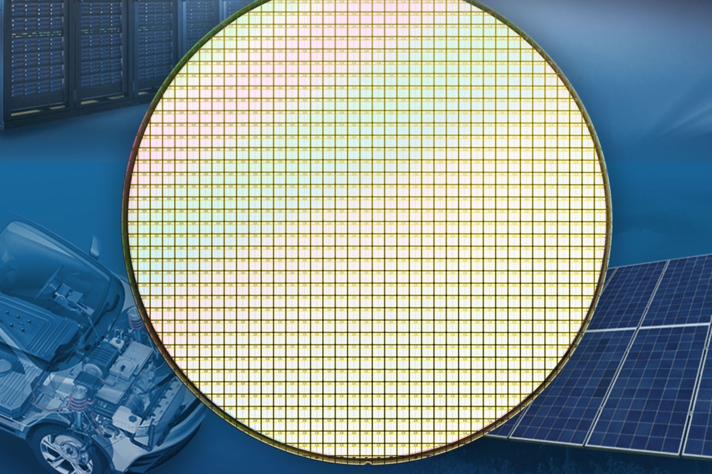
Compound semiconductors are widely used in RF applications. In millimetre-wave front-ends, the GaAs pseudomorphic HEMT, known simply as the pHEMT, combines exceptional performance with an adequate breakdown voltage, strengths that ensure it’s long been used in wireless backhaul amplification in the E-band. GaAs pHEMT power amplifiers (PAs) are also widely deployed in aerospace/defence systems, optical transceivers and low earth-orbit satellites (see Figure 1).
Due to the increasing popularity of massive data transmission, there is increasing demand for an expansion in spectral resource that can satisfy this explosive traffic growth. This has already led to the exploration of opportunities in both the W-band, which spans 75 GHz to 110 GHz, and the higher frequency D-band, at around 130 GHz to 175 GHz.
One prominent example of the commercial pursuit of using such bands is Nokia’s construction of the world’s first live full duplex D-band link, for mobile backhaul, announced in 2024. There are also low earth orbit applications, such as SpaceX’s Starlink. This company has been granted permission by the Federal Communications Commission to upgrade its constellation to 12,000 second-generation satellites equipped with W-band technology. However, despite enjoying market dominance in the past, the GaAs pHEMT is not the leading candidate for these commercial applications.

Figure 1. Communication transmission application
architecture of (a) mobile wireless backhaul, (b) a low-earth orbit satellite,
and (c) optical transceivers in a data centre.
The biggest barrier to the adoption of GaAs pHEMTs in W and
D-band applications is the gain of these transistors. According to current
research, only a few GaAs pHEMTs are being used in the D-band, due to the rapid
degradation of gain with increasing operating frequency. Moreover, InP HBTs and
GaAs metamorphic HEMTs (mHEMTs) are more compelling, due to higher maximum
available gain in the D-band region. However, both these rivals are held back
by a relatively low operating voltage, due to the inherently low breakdown
voltage, which limits output power and reliability. To fulfil these
requirements related to gain, to output power and to reliability, our team at
WIN Semiconductors Corporation has developed a 70 nm GaAs pHEMT for W- and
D-band PA applications.

Figure 2. Cross-section diagram of both active and passive
components of technology.
Device fabrication…
Our latest generation of GaAs pHEMT technology employs a
gate length of 70 nm, a significant reduction over its predecessor, which had a
100 nm gate length. For both classes of device, epiwafers are produced by
loading 6-inch GaAs substrates in an MOCVD reactor. Growth in this chamber
begins with a buffer, and is followed with an InGaAs channel, an AlGaAs
Schottky layer, an AlAs etching stop layer, and an n-type doped
GaAs cap layer. Subsequent processing requires a more complicated
manufacturing process flow for the pHEMTs with a shorter gate length.
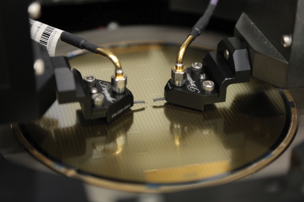
For these devices, fabrication begins by forming Ohmic source and drain contacts. Ion implantation follows, enabling device isolation. The next step is the most critical – using electron-beam lithography to define a 70 nm T-shaped gate, which has an asymmetric gate-to-drain recess length. After this, we undertake back-end-of-line processing, which includes the addition of two interconnect metal layers and a SiNx film to fabricate the capacitors. To minimise the parasitic capacitance between two metal layers, we form air-bridge crossovers with a top metal layer with a thickness of 4 mm. Our final step is to thin the substrate down to 50 mm and then add a backside via and a backside plating metal (see Figure 2 for a cross-sectional diagram of the active and passive components).
… and characteristics
Device characteristics determine whether our 70 nm GaAs pHEMT technology can be used for W- and D-band operation, and in
particular whether these devices deliver sufficient gain and output power. The
major aim of our 70 nm GaAs pHEMT development programme has been to enhance
gain performance, while maintaining the output power provided by 100 nm GaAs
pHEMTs.
According to DC characteristics, shrinking the gate length from 100 nm to 70 nm trims the on-state resistance by 21.6 percent, falling from 0.83 Ω mm to 0.65 Ω mm (see Figures 3 (a)). Transfer characteristics, using a drain voltage of 4 V, determine that our 70 nm GaAs pHEMT produces a maximum drain current of 701 mA mm-1 at a 0.5 V gate voltage, and has a D-mode threshold voltage of -0.97 V (see Figure 3 (b)). Peak transconductance is 760 mS mm-1 at a -0.16 V gate voltage, implying that the device is behaving in an appropriate manner, and can operate with a negative gate voltage. This is an attractive feature, reducing design complexity for circuit designers, who can simply use a different negative bias voltage to turn-on and to turn-off the transistor.

Figure 3. DC characteristics of (a) output and (b) transfer
characteristics for 70 nm GaAs pHEMT.
As our 70 nm HEMT has similar values for the maximum drain current, threshold
voltage and peak transconductance as its cousin with the 100 nm gate length, we expect the scaled device to deliver a similar output power.
For millimetre-wave PA applications, the cut-off frequency (ft) and maximum oscillation frequency (fmax) are great metrics for predicting the current gain and power gain, respectively, of the pHEMT. We use our pHEMT with a symmetric gate recess undercut to evaluate the relationship between the gate length, and both the cut-off frequency and the maximum oscillation frequency (see Figure 4). Scaling the gate length from 120 nm to 70 nm increases the cut-off frequency by more than 10 percent, but only delivers a slight increase in the maximum oscillation frequency, due to an increase in device access resistance. As power gain is a key characteristic for PA applications, it makes sense for us to slightly reduce the recess undercut on the source side, a modification that trims resistance and increases the maximum oscillation frequency.
We have also evaluated the maximum available gain and the output power of our 70 nm pHEMTs, using a drain voltage of 4 V, a drain current of 300 mA mm-1, and a 2 × 25 μm device with a microstrip waveguide (see Figure 5). Compared with its cousin with a 100 nm gate length, our 70 nm pHEMT produces a higher maximum available gain across the D-band, with a minimum gain of 7.5 dB at 145 GHz, and 8 dB at 175 GHz. There is an increase in maximum available gain of 4.8 dB at 175 GHz, enabling the 70 nm GaAs pHEMT to support D-band PA applications
It’s possible to adjust the operating voltage to trade one characteristic against another, and optimise amplifier design for a particular application. For example, when pHEMTs are used in optical transceivers, the operating bias is lower than mobile backhaul PAs, and the maximum available gain can be further increased by reducing drain bias. This point is illustrated in Figure 6, which plots the maximum oscillation frequency, and the frequency at a stability factor of 1, for our 70 nm GaAs pHEMT under different values for the drain bias. Lowering this bias to 2 V enhances the maximum oscillation frequency to 417 GHz, and should ensure a higher maximum available gain.

Figure 4. Correlation between the cut-off frequency (ft), and the maximum oscillation frequency (fmax) and the gate length (Lg), based on a device with symmetric gate recess.
After this analysis of the small signal performance, we
measured the large signal characteristic of our 70 nm device. According to a
preliminary load-pull test, using a drain voltage of 4 V and a drain current of
300 mA mm-1, our device produces an output power of 15.44 dBm
(700 mW mm-1) and a power-added efficiency of 47.8 percent at
29 GHz. These values are similar to those for the 100 nm pHEMT, a finding we
attribute to similar figures for the maximum drain current and the threshold
voltage. Our view is that the slight reduction in power-added efficiency for
the 70 nm device is due to the matching impedance we employed. The conclusion
we would draw from these results is that reducing the gate length of the pHEMT
to 70 nm improves high-frequency operation, with higher gain realised, without
detriment to the output power.

Figure 5. RF characteristics. (a) The ratio of maximum
stable gain (MSG) to maximum available gain (MAG), and (b) load-pull test for
70 nm GaAs pHEMT.
As well as impressive performance figures, a high level of
reliability is crucial for commercialisation. We have evaluated this aspect of our device with an Arrhenius plot of time-to-failure, using a drain bias of 4.4 V and a drain
current of 330 mA mm-1, which is 10 percent higher than the
maximum operation bias condition (see Figure 7). Defining device failure as a
20 percent degradation in drain current at a gate voltage of 0.4 V, values for
the mean-time-to-failure and 1,000 defect-parts-per-million are 6.76 × 10⁶ hrs
and 2.70 × 10⁶ hrs, respectively, at a junction temperature of 125 °C. Activation energy is 1.81
eV.

Figure 6. Correlation of the maximum oscillation frequency
(fmax) and frequency for a stability factor, K, of 1, as a function of the
drain voltage.
Based on our characterisation, there is much to like about
our 70 nm GaAs pHEMT, which combines a high maximum available gain with a high
output power when operating at a drain bias of 4 V. We attribute these
exceptional characteristics primarily to the short gate length and the
asymmetric structure. While yield control is very challenging for manufacturing
a device with a narrow gate length, it’s an obstacle we’ve overcome, realising
robust gate yields of more than 97 percent for 70 nm pHEMTs produced from
6-inch GaAs wafers. These strengths, alongside impressive device lifetimes,
provide the proof that we are offering an attractive foundry service for W- and
D-band PAs with our new 70 nm GaAs pHEMT technology.

Figure 7. Reliability test result of 70 nm pHEMT.