Berkeley team makes atomically thin light emitter

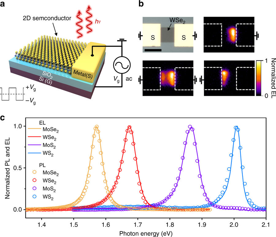
UC Berkeley engineers in California have built a bright-light emitting device that is millimetres wide and fully transparent when turned off. The light emitting material is a monolayer compound semiconductor WSe2, a transition-metal dichalcogenide (TMDC).
The device opens the door to invisible displays on walls and windows - displays that would be bright when turned on but see-through when turned off - or in futuristic applications such as light-emitting tattoos, according to the researchers.
"The materials are so thin and flexible that the device can be made transparent and can conform to curved surfaces," said Der-Hsien Lien, a postdoctoral fellow at UC Berkeley and a co-first author along with Matin Amani and Sujay Desai, both doctoral students in the Department of Electrical Engineering and Computer Sciences at Berkeley.
Their study was published March 26 in the journal Nature Communications. The work was funded by the National Science Foundation and the Department of Energy.
The device was developed in the laboratory of Ali Javey, professor of Electrical Engineering and Computer Sciences at Berkeley. In 2015, Javey's lab published research in the journal Science showing that monolayer semiconductors are capable of emitting bright light, but stopped short of building a light-emitting device.
This device is a proof-of-concept, and much research still remains, primarily to improve efficiency. Measuring this device's efficiency is not straightforward, but the researchers think it's about 1 percent efficient. Commercial LEDs have efficiencies of around 25 to 30 percent.
The concept may be applicable to other devices and other kinds of materials, the device could one day have applications in a number of fields where having invisible displays are warranted. That could be an atomically thin display that's imprinted on a wall or even on human skin.
"A lot of work remains to be done and a number of challenges need to be overcome to further advance the technology for practical applications," Javey said. "However, this is one step forward by presenting a device architecture for easy injection of both charges into monolayer semiconductors."
'Large-area and bright pulsed electroluminescence in monolayer semiconductors' by Der-Hsien Lien et al; Nature Communications 9, Article number: 1229 (2018)
The picture above shows a) an AC voltage is applied between the gate and source electrodes and emission occurs near the source contact edge. b Optical and EL image of a WSe2 device, showing that emission is only observed near the grounded source contacts. Scale bar is 10"‰Î¼m. c EL and PL spectra measured for MoSe2, WSe2, MoS2, and WS2 monolayer devices.


