Double heterostructure HEMTs for handsets

A collaboration of engineers based in Singapore claims to have broken new ground by investigating the potential of a double heterostructure design for low-voltage GaN-on-silicon HEMTs.
These researchers argue that this class of transistor is a compelling candidate for power amplification in the 5G Frequency Range 2 band – this is defined as more than 24 GHz, and features a number of bands more than three times as wide as those found below 6 GHz. As a rule of thumb, the maximum data rate from any band is proportional to its width, making the double-heterostructure HEMT an attractive option for high-speed uplinks and downlinks.
Up until now, efforts at investigating GaN devices operating at low voltages, an essential requirement for deployment in handsets, have been limited single heterostructures. Meanwhile, the development of double-heterostructure devices, which offer excellent carrier confinement and enable a high mobility and a high saturation velocity, has only occurred at higher voltages.
Strengths of the double-heterostructure devices, made by engineers at Nanyang Technical University, A*STAR, the Singapore-MIT Alliance for Research and Technology, and the National University of Singapore, include a record-breaking saturated output power for low-voltage GaN-on-silicon HEMTs operating in the 5G Frequency Range 2 band.
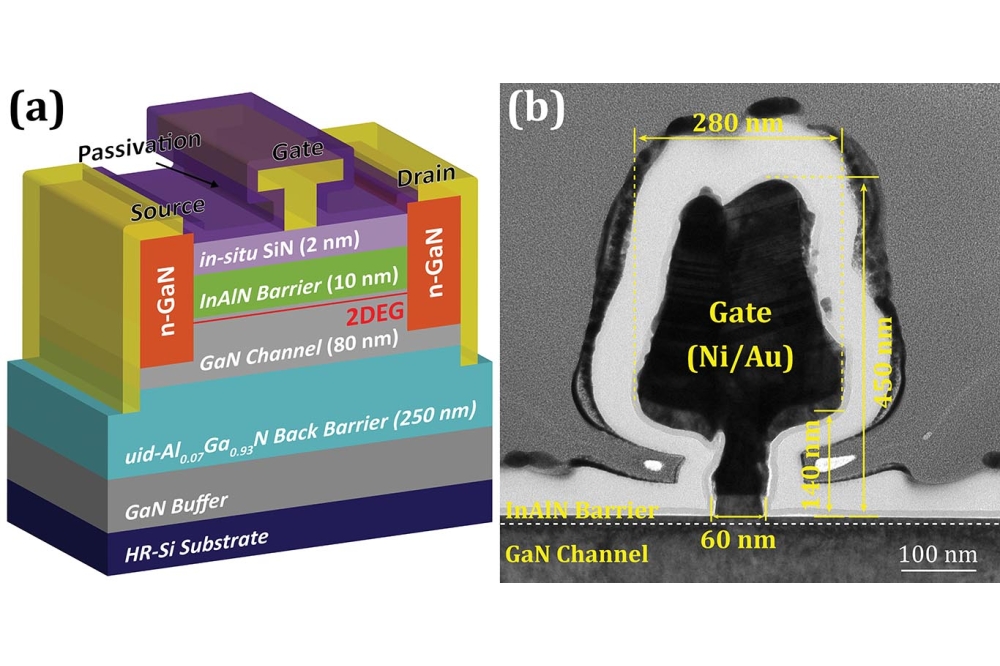
Fabrication of this team’s HEMTs began by loading a high-resistivity silicon substrate into an MOCVD chamber and depositing a 1 µm-thick GaN buffer, followed by a 150 nm-thick AlGaN back barrier, a 180 nm-thick GaN channel, a 5 nm-thick top barrier, and a 5 nm-thick SiNx layer. According to Schrödinger-Poisson calculations by the engineers, this double heterostructure ensures a significantly better carrier confinement than a single heterostructure.
Processing of the epiwafer into devices involved the addition of Ti/Al/Ni/Au ohmic contacts, device isolation by mesa etching, the addition of Ni/Au T-shaped gates, and passivation realised by atomic layer deposition of a 10 nm-thick layer of Al2O3.
Measurements on these transistors, which have a gate length of 120 nm, gate-source and gate-drain spacings of 690 nm, and a source-to-drain spacing of 1.5 µm, revealed a maximum drain current of 1.9 A mm-1, an on-resistance of 1.5 Ωmm, and a maximum transconductance of 0.66 S mm-1. The cut-off frequency of the HEMT is 145 GHz, and the maximum oscillation frequency 195 GHz.
Large-signal performance, evaluated at 30 GHz and 5 V and involving the use of on-wafer load-pull measurements, determined a saturated output power of 1.3 W mm-1 (16.12 dBm), with an associated power-added efficiency of 32 percent and a gain of 3.7 dB.
Leader of the team, Geok Ing Ng, told Compound Semiconductor that the dimensions of their HEMTs are in the right ball-park for use in handsets.“We believe a gate length of 100 nm to 120 nm would satisfy practical millimetre-wave handset applications. This is considering the transistor’s short-channel effects, fabrication complexity and yield, among other factors.”
However, he says that there are no obstacles to lateral scaling of these transistor, to improve performance at higher frequencies, such as the W-band. “We used the term ‘aggressive scaling’ to generically refer to lateral scaling. Notably the source-drain spacing – currently 1.5 µm – could be reduced.”
One of the team’s next goals is to conduct a comprehensive study of low-voltage millimetre-wave GaN-on-silicon HEMTs, considering epitaxy and device design. “Through aggressive lateral scaling of the transistor, we hope to explore the performance limits of GaN-on-silicon HEMTs at higher frequencies, such as the W-band.”
Another aim is to go beyond simply focusing on the output power of the HEMT and start looking at other specifications, such as linearity, an important metric for the RF front-end.
Reference
H. Li et al. IEEE Electron. Dev. Lett.