Loading...
News Article

AlixLabs to collaborate with Linköping University

News
Swedish startup to enter joint research in GaN and InN deposition and etch

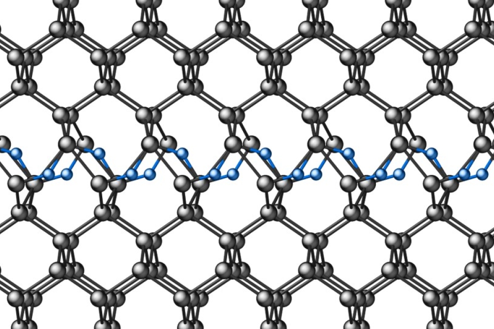
AlixLabs AB, a Swedish semiconductor startup specialising in Atomic Layer Etching (ALE), announces that it has entered a research collaboration with Linköping University. The company and the university will join forces in furthering Swedish research into GaN and InN deposition and etch.

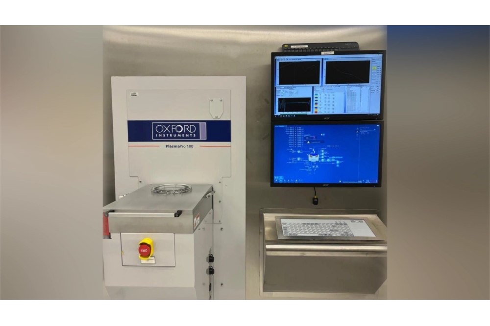
“Our goal is to widen our research portfolio beyond deposition to etching, which is AlixLabs’ specialty,” says Henrik Pedersen, professor in inorganic chemistry at Linköping University. “During our initial research phase, we found that we have the same plasma etch equipment in our university labs as AlixLabs has at its home base in Lund, meaning we can run research in parallel. We look forward to exchanging information and know-how, especially in an all-Swedish collaboration.”

The resulting research will help strengthen AlixLabs’ offering within RF and power semiconductors, a field the EU has labeled as critical for its climate goals. It is a participant in the GaN-centreed, Infineon-led, All2GaN project which underpins the union’s ambitions to achieve climate neutrality by the year 2050.

“We are excited about partnering up with the team at Linköping University and Professor Pedersen, a renowned researcher in the atomic layer deposition (ALD) and semiconductor chemistry space. Our goal is to find ways to qualify our processes for use in materials beyond silicon and we found significant synergies between our labs with regards to GaN and InN,” says Jonas Sundqvist, CEO and co-founder of AlixLabs.

“Our etching processes have found a lot of interest among clients in the power electronics field. Ideally, our processes will have something to offer all players, no matter which semiconductor material they wish to process,” concludes Sundqvist.

EU invests €15M to help firms use photonics
ST and Innoscience sign GaN deal
Lumentum shows InP advances at OFC
A step towards higher DUV LED efficiency
Quantum Science achieves ISO 9001:2015 certification
Ascent wins order for power-beaming module
Navitas Partners with Great Wall for 400V-DC power
SemiQ supplies SiC MOSFET modules for EV battery cell cyclers
Coherent and Keysight collaborate on 200G/lane multimode VCSEL tech
Lumentum and Marvell exhibit integrated 450G optical interface
Marktech announces new MWIR LEDS
Imec identifies stable range for GaN MISHEMTs in RF PAs
Polar Light completes $3.4m funding round
Lynred launches advanced thermal imaging modules
Altum RF expands Sydney design centre
Sivers announces partnership with O-Net
Ayar Labs unveils first UCIe optical chiplet
Aixtron delivers InP tool to Nokia
WHU-USTC team demo novel GaN chip temperature monitoring
Phlux lands £9m to take InGaAs sensors to next level
4-inch gallium oxide facility established in Swansea
Mazda and Rohm collaborate on automotive GaN
University of South Carolina chooses MOCVD tool from TNSC
Wolfspeed appoints new CEO amidst funding crisis
SiC slowdown is only short term, says Yole
Pragmatic launches flexible IGZO-based NFC chip
Poet ships latest optical engine samples
EU project to develop 1200V DC powertrain
£250m to turbocharge Welsh compound semi cluster
Scientists harness phonon-polariton electroluminescence
TU Graz team reveals the secrets of heat conduction
Aixtron to partner in ‘GraFunkL‘ UVC project
×
Search the news archive

To close this popup you can press escape or click the close icon.
Logo
x
Logo
×
Register - Step 1

You may choose to subscribe to the Compound Semiconductor Magazine, the Compound Semiconductor Newsletter, or both. You may also request additional information if required, before submitting your application.


Please subscribe me to:


You chose the industry type of "Other"

Please enter the industry that you work in:
 
x
Adblocker Detected
Please consider unblocking adverts on this website