
Multi-junction cell converts third of sunlight into electricty
Fraunhofer ISE and EV Group develop highly efficient solar cell by combining GaInP, GaAs and silicon
Researchers at the Fraunhofer Institute for Solar Energy Systems ISE together with the company EV Group (EVG) have developed a new silicon and III-V semiconductor- based multi-junction solar cell, which can convert exactly one-third of the incident sunlight into useful electricity. This result is now published in Nature Energy.
The Fraunhofer researchers achieved the high conversion efficiency of the silicon-based multi-junction solar cell with extremely thin 0.002 mm semiconductor layers of III-V compound semiconductors, bonding them to a silicon solar cell.
The visible sunlight is absorbed in a GaInP top cell, the near infrared light in GaAs and the longer wavelengths in the silicon subcell. In this way, the efficiency of silicon solar cells can be significantly increased.
"Photovoltaics is a key pillar for the energy transformation," says Andreas Bett, institute director of Fraunhofer ISE. "Meanwhile, the costs have decreased to such an extent that photovoltaics has become an economically viable competitor to conventional energy sources. This development, however, is not over yet. The new result shows how material consumption can be reduced through higher efficiencies, so that not only the costs of photovoltaics can be further optimised but also its manufacture can be carried out in a resource-friendly manner."
Already in November 2016, the solar researchers in Freiburg together with their industry partner EVG demonstrated an efficiency of 30.2 percent, increasing it to 31.3 percent in March 2017. Now they have succeeded once again in greatly improving the light absorption and the charge separation in silicon, thus achieving a new record of 33.3 percent efficiency. The technology also convinced the jury of the GreenTec Awards 2018 and has been nominated among the top three in the category 'Energy'.
The technology
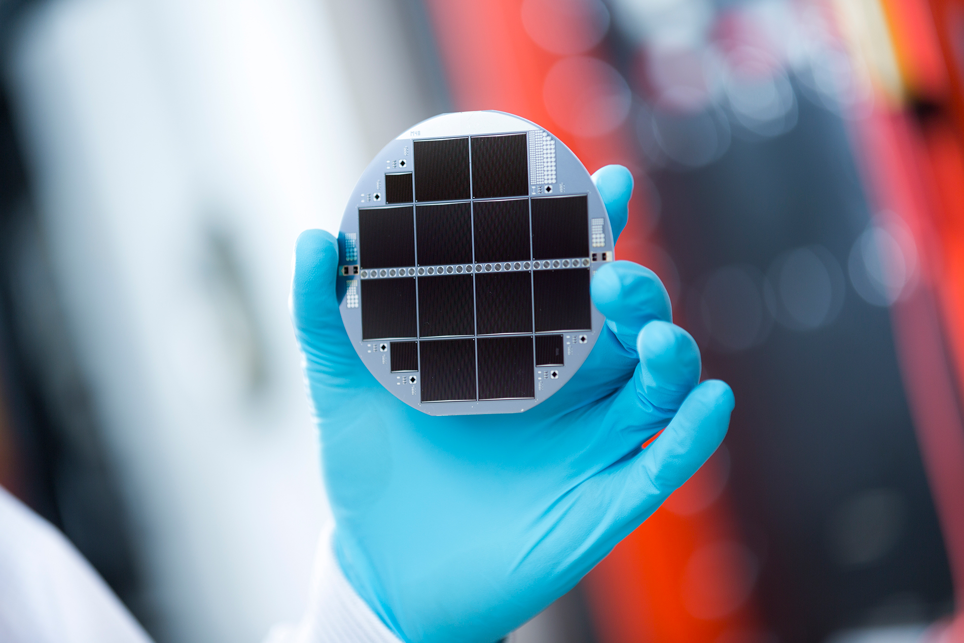
For this achievement, the researchers used "direct wafer bonding" to transfer III-V semiconductor layers, of 1.9 micrometers thick, to silicon. The surfaces were deoxidized in a EVG580 ComBond chamber under high vacuum with a ion beam and subsequently bonded together under pressure. The atoms on the surface of the III-V subcell form bonds with the silicon atoms, creating a monolithic device. The complexity of its inner structure is not evident from its outer appearance: the cell has a simple front and rear contact just as a conventional silicon solar cell and therefore can be integrated into photovoltaic modules in the same manner.
The III-V / Si multi-junction solar cell consists of a sequence of subcells stacked on top of each other. Tunnel diodes internally connect the three subcells made of GaInP, GaAs and silicon, which span the absorption range of the sun's spectrum. The GaInP top cell absorbs radiation between 300 and 670 nm. The middle GaAs subcell absorbs radiation between 500 and 890 nm and the bottom Si subcell between 650 and 1180 nm, respectively.
The III-V layers are first epitaxially deposited on a GaAs substrate and then bonded to a silicon solar cell structure. Here a tunnel oxide passivated contact (TOPCon) is applied to the front and back surfaces of the silicon. Subsequently the GaAs substrate is removed, a nanostructured backside contact is implemented to prolong the path length of light. A front side contact grid and antireflection coating are also applied.
On the way to the industrial manufacturing of III-V / Si multi-junction solar cells, the costs of the III-V epitaxy and the connecting technology with silicon must be reduced. There are still great challenges to overcome in this area, which the Fraunhofer ISE researchers intend to solve through future investigations. Fraunhofer ISE's new Centre for High Efficiency Solar Cells, presently being constructed in Freiburg, will provide them with the perfect setting for developing next-generation III-V and silicon solar cell technologies. The ultimate objective is to make high efficiency solar PV modules with efficiencies of over 30 percent possible in the future.
Project Financing
Roman Cariou, the young scientist and first author, was supported through the European Union with a Marie Curie Stipendium (HISTORIC, 655272). The work was also supported by the European Union within the NanoTandem project (641023) as well as by the German Federal Ministry for Economic Affairs and Energy BMWi in the PoTaSi project (FKZ 0324247).


