
Tuning of 2D materials relies on defects
Penn State study shows that defects can enhance a material's physical, electrochemical, magnetic, energy and catalytic properties
Perfection is not everything, according to an international team of researchers whose 2D materials study shows that defects can enhance a material's physical, electrochemical, magnetic, energy and catalytic properties.
"Electronic devices, like transistors, are usually made from relatively bulky stacked layers of metal, oxides and crystalline semiconductors," said Shengxi Huang, assistant professor of electrical engineering, Penn State. "We would like to make them with 2D so that they can be faster, smaller and more flexible.
To do this, the researchers are looking at MoS2 single atomic layers. They report the results of their investigation in a recent issue of ACS Nano.
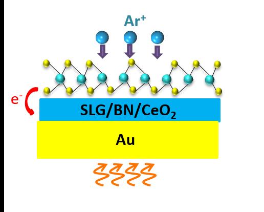
MoS2 is a molecule made up of one molybdenum atom with two sulphur atoms attached. The molecules line up with the molybdenum in the middle and the sulphur atoms on the top and bottom when forming a 2D, single-layer, film. These films were placed on a variety of substrates - gold, single-layer graphene, hexagonal boron nitride and cerium dioxide -and irradiated to create defects in the lattice structure.
Creating 2D materials is not a perfect manufacturing process and defects are always present in the lattice. The researchers wanted to determine how those defects changed the physical and electrochemical properties of the MoS2. Irradiation causes some of the MoS2 to lose a sulphur atom from the surface. Using these less-than-perfect films, the researchers could see how the materials changed using a variety of microscopies and spectroscopies.
Simulations of lattice defects allowed the researchers to manipulate the materials and produce structures that matched the experimentally defective films. They found that the materials properties results of their simulations matched their experimental results.
"We found that the sulphur defects improved the physical characteristics of the material," said Huang. "By choosing the locations and number of defects, we should be able to tune the material's band structure, improving its electronic capabilities."
Experimentally, the researchers found that many more sulphur atoms are lost than molybdenum atoms, because the sulphur is on the surfaces and the molybdenum is protected in the middle. They also noted that because so many sulphur atoms leave the material, the defects caused by the absence of sulphur overwhelm any effect the absence of a molybdenum in the lattice might have.
Investigating how different substrates enhanced or did not enhance the properties of the two-dimensional material, the researchers found that "the substrates can tune the electronic energy levels in MoS2 due to charge transfer at the interface." The material properties of the substrate also change the properties of the two-dimensional single layer. Cerium dioxide, because it is an oxide, altered the electrical properties of the material differently than the other substrates.
Smaller, faster and more flexible electronics are not the only possible outcome of tuning these 2D materials.
"If we have the right amount of sulphur vacancies, we can enhance chemical processes like hydrogen evolution from water," said Huang. Huang refers to the splitting of water, a process used to create gaseous hydrogen and oxygen from liquid water where properly defective MoS2 could enhance the process and reduce the amounts of energy and costs needed and increase the amount of hydrogen produced.
Molybdenum is a transition metal and other members of this atomic group also form molecules called dichalcogenides. These include tungsten, niobium, zirconium, titanium and tantalum and they form layers with sulphur and other chalcogenides such as selenium and tellurium. Other dichalcogenides can be made into 2D materials and may also be tunable to enhance their properties.


