
2D CdTe makes spontaneous origami
Spontaneous folding of ultrathin CdTe sheets produces perfect nano-sized scrolls
A team of scientists from Lomonosov State University (MSU) together with international colleagues have discovered that t2D sheets of CdTe can spontaneously fold into nanoscrolls. This effect may be used in electronics and photonics. The results of the study were published in Chemistry of Materials journal.
In the course of the study the team focused on 2D semiconductor materials. Among others, they include graphene, phosphorene, 2D layers of MoS2, and 2D perovskites. These materials are one atom thick crystals with 2D electronic properties. Researchers believe that they may be used for the development of new devices.
"We studied 2D CdTe and discovered an unexpected effect of spontaneous folding of its ultrathin (only 1 nm) sheets that are also called colloidal quantum wells," said Roman Vasiliev, a co-author of the work, PhD of Chemical Sciences, and Associate Professor of the Faculty of Chemistry and the Faculty of Materials Science, MSU.
Colloidal quantum wells are a new generation of colloidal quantum dots. Quantum dots are distinguished by their luminescent properties and are used in commercial devices, such as TV sets. Quantum wells, a 2D type of quantum dots, are being studied today, but we already know that they possess very narrow luminescence bands, which is important for bright color rendering in light-emitting devices.
The team studied the properties of 2D sheets of CdTe by exchanging organic molecules attached to their surface and securing the stability of nanoparticles. In order to synthesise 2D CdTe the scientists used the colloidal method and obtained them in a flask. To do so, the scientists initiated a reaction of obtaining CdTe nanoparticles in an organic solvent in the presence of surfactants. By changing the conditions of the reaction they managed to cause the particles to grow into one nanometer thick sheets.
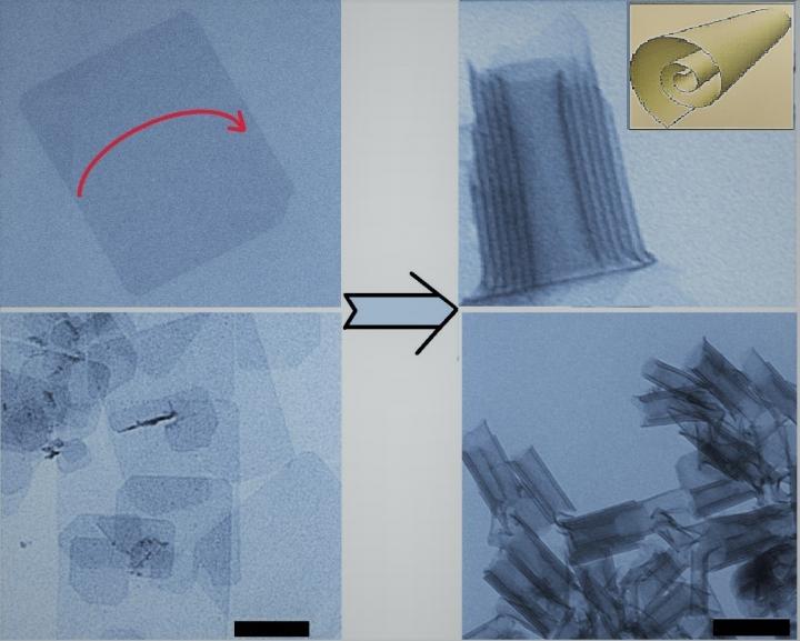
At first the authors of the work grew flat 2D sheets covered with oleic acid as a stabiliser. They managed to obtain sheets with length reaching hundreds of nanometers and thickness of strictly one nanometer. After that the team started replacing the molecules of oleic acid with other organic molecules and analysing sizes and shapes of the obtained nanoparticles, as well as their composition and crystal structure. At this stage they used a transmission electron microscope of MSU Shared Knowledge Center.
In the course of the study the team discovered that when a specific type of stabilisers (thiols) is used, flat sheets of CdTe suddenly fold into perfect scrolls. When attached to the surface of a sheet, thiol molecules increase its thickness by one monolayer (0.15 nm) and cause mechanical stresses making the sheet to fold in a certain crystallographic direction. The folding takes place for all nanoparticles at once, and the radius of the fold is the same for all nanostructures.
"The study opens new prospects for manipulations with 2D materials and nanoparticles. The folding effect came as a surprise for us. It resembles the process of making origami, but in this case the sheets are one nanometer thick. Knowing how to change spatial shape of nanoparticles, we could use them in the manufacturing of optic materials with anisotropic behavior and polarised luminescence. We could create active light-emitting matrices for displays that would reduce energy consumption and increase brightness and intensity of various devices. Perhaps, we could also develop new nano-devices, for example, tube-shaped transistors. These interesting properties may be of use in new generations of light-emitting and sensor devices, as well as in optic and optoelectronic technologies and nanotechnologies," concluded the scientist.


