
Photonics ICs prepped for market
Intengent, GCS and VLC Photonics have joined forces to deliver an InP PIC platform for industrial-grade wafer fabrication. Rebecca Pool finds out more. [Image: GCS-Intengent-VLC Consortium]
Earlier this year, Canada-based III-V photonics consultancy, Intengent, joined forces with US compound semiconductor wafer fabrication foundry, Global Communication Semiconductors, and photonics IC design house, VLC Photonics, from Spain, to take InP photonic IC development to commercial production.
Together the partners will offer fabless development for the production of customised InP PICs, and Intengent chief executive, Valery Tolstikhin, is certain that the new team has what it takes to deliver a generic InP PIC platform for industrial-grade wafer fabrication.
As he points out, GCS is one of the world's biggest III-V commercial foundries, churning out InP, as well as GaAs and GaN wafers, for RF electronics and optoelectronics markets in large volumes.
Meanwhile, Tolstikhin himself, has pioneered a re-growth-free photonic integration platform - Taper Assisted Vertical Integration - based on the GCS's well established optoelectronics process, for designing and developing InP PICs.
Factor in the VLC Photonics' design library and process design kit expertise, which is already applied to other commercial PIC platforms and can slash PIC design effort and risk, and Tolstikhin's confidence becomes understandable.
"Typically, people in the industry have an idea of the application they want to serve but often, don't know what device they want," highlights Tolstikhin. "So we can conceptualize the PIC that matches that application and develop it through regular design-manufacturing-verification cycles - that's what we do as a Consortium."
"Intengent provides the integration platform and underlying epitaxy design, VLC brings a wealth of experience in PIC design and characterisation, and GCS is probably the biggest commercial foundry in the III-V photonics domain," he adds. "I have seen optics increase from 5% of GCS's overall volume to more than 50%; this is a huge change and this [one-stop shop for InP PICs] is something I have wanted to be part of for a long time."
Early days
In the last two decades, Tolstikhin has launched several PIC-based businesses, pioneering various photonic integration platforms based on different versions of vertical integration.
He first became involved with PICs in 2000, when he joined MetroPhotonics, a spin-off from the National Research Council of Canada, set up to commercialise wavelength-division multiplexing technology for InP. Here, he led PIC design until the company folded in 2005, and during this time developed and patented a robust, regrowth-free active-photonic device integration technique called 'Single-Mode Vertical Integration'.

Tolstikhin hopes to see 'real commercial infrastructure' for the fabless development of III-V photonics, in place within five years. [Intengent]
Having developed a number of InP-based WDM components at MetroPhotonics, he went onto launch OneChip Photonics, with a view to developing cost-efficient InP PICs using his regrowth-free PIC technology.
The OneChip business model was based on fabless manufacturing, which Tolstikhin has always touted as being appropriate for low volume markets. And during his leadership at OneChip, he honed his vertical integration process, pioneering 'Multi-Guide Vertical Integration'.
Here, by vertically stacking the necessary materials for, say, lasers and detectors, the technology allowed the company to monolithically integrate active, as well as passive, devices onto the same substrate in a single epitaxial growth step.
As the chief executive highlights: "I individually designed every single epitaxial structure for every PIC product developed or tried by OneChip, which was an absolutely crucial step in regrowth-free PIC production."
OneChip went onto develop PIC-based optical interconnects for 100G datacentre market applications, partnered with GCS and IQE on wafer processing and epitaxial growth but closed in 2014, by which time Tolstikhin had co-founded ArtIC Photonics, a fabless developer of InP-based PICs for telecoms and datacoms markets.
ArtIC remains today, designing PIC chips for optical component products, but in 2015 Tolstikhin founded Intengent to design and develop InP PICs, this time based on Taper Assisted Vertical Integration (TAVI).
Building blocks
The TAVI library comprises many building blocks, from lasers to amplifiers to detectors on the active device side and splitters/combiners, filters, and various elements of waveguide circuitry, on the passive device side. What is common to all of them is a lateral taper assisted adiabatic transition between vertically stacked and functionally different guiding layers.
Perhaps, the most generic building block, which showcases the TAVI platform from this prospective, is the spot-size converter that permits the transition of guided light from a PIC waveguide to an optical fibre. This is defined by building lateral tapers in a specially designed multilayer epitaxial structure. Indeed, as Tolstikhin points out: "Intengent has now been working with a commercial foundry on the epitaxy growth of specialised wafer designs that comprise up to 90 layers."
"It is so important to allow the optical signal to move from one vertical layer to another.... and lateral tapering allows you to vertically connect all of your waveguides," he adds. "This method is very flexible, it is a big deal and we are seeing big gains in reliability."
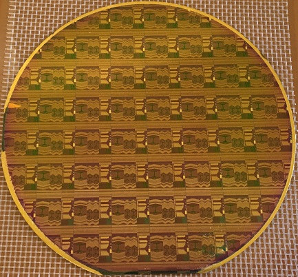
Right now, Intengent is predominantly working on four inch wafer sizes with GCS, but intends to transition to six inch wafers as soon as possible.
"I would love to work with six inch, even eight inch wafer sizes but these are not readily available right now," says Tolstikhin. "In terms of cost, size of wafers really does matter here as the number of devices you can harvest is so different from wafer to wafer; this is not like laser development, these really are big chips."
"I cannot name the date, but six inch wafer fabrication is coming," he adds.
Crucially, so is demand. According to Tolstikhin, he is thinking of expanding the company to cope with growing demand for InP-based PICs from various segments of the market, from tele- and Datacom to microwave photonics and quantum inscription.
And at the moment, the chief executive is also seeing interest from silicon photonics businesses demanding III-V integration. "[Designs] now need sophisticated light sources that cannot be provided by off-the-shelf by bulk assembly," he says. "This is one avenue that wasn't really evident a few years ago."
With demand rising, Tolstikhin is now looking forward to seeing what he describes as 'real commercial infrastructure' for the fabless development of III-V photonics. He hopes such infrastructure will be in place within the next five years, and importantly, he expects this to be able to provide a full level of customisation, within a reasonable budget.
"Following the development of silicon photonics, many in our industry now understand the need for fabless development and the pointlessness of building an entire infrastructure for just one device," he asserts. "We are trying to capitalise on this and provide the services that those people want."


