
Growing III-V on glass
A textured film of MgO promises to enable the growth of III-V devices on large glass sheets by Ashok Chaudhari from Solar-Tectic
Is silicon a superior substrate to sapphire for making GaN-based LEDs? Well, some companies certainly think so. Take Plessey Semiconductors of the UK: it has argued that silicon has the upper hand not only in cost, but also in thermal attributes. Meanwhile, Samsung of South Korea claims that cost savings could be as high as 60 percent, by combining 200 mm GaN-on-silicon epiwafers with wafer-level, chip-scale packaging. That's a view shared by Allos of Germany, which thinks that these cost savings could eventually be even more substantial, as the process matures.
At Solar-Tectic LCC of Briarcliff Manor, NY, we applaud the move away from costly sapphire wafers. But we think it's possible to go even further, and make even greater savings. Our idea is that instead of using a silicon wafer, GaN can be grown on a thin film of silicon or germanium. So production then involves taking a cheap substrate, such as soda-lime glass, and depositing on this a thin film of silicon (or germanium), and following it up with the growth of a GaN LED heterostructure. As well as slashing substrate costs, this approach could deliver another key advantage for the manufacture of microLEDs: the devices could be made monolithically, without the transfer of pixels, since GaN can be grown directly on the silicon film.
We expect that our approach will arouse some skepticism within the compound semiconductor community, which sees highquality heterostructures as the bedrock for successful devices. It is clear that with our approach, a polycrystalline film of silicon is not acceptable. But how much better does it need to be? If it is not exactly single crystal, but close, is that good enough?
There are those in the materials community that have been wrangling with these questions for decades. Through their efforts, they have realised that the silicon film must have a "˜preferential orientation' or a "˜texture'. One way to accomplish this is to produce a thin buffer layer on a highly textured surface of glass. By adopting this approach, texture or orientation can be introduced in the silicon film. This holds the key to creating a textured silicon film that would be close enough to a single crystal silicon wafer in quality that device performance would be equal. On this film, oriented III-V materials for LEDs could then be grown heteroepitaxially.
We accept that there is a compromise with this approach: the removal of the thermal advantage associated with silicon, which has a much higher conductivity than soda-lime glass. However, that's not a big issue for the display industry, because the manufacture of displays often involves a processing step that deposits crystalline silicon thin-film on buffered glass, known as low temperature polysilicon (LTPS). Alternatively, an amorphous(a-Si:H) silicon thin-film is deposited by plasma-assisted CVD. The latter is the most common method used today.
Outweighing this minor drawback, the inferior thermal conductivity, there is virtually no limit to substrate size with our crystalline silicon thin-film approach. It is only the reactor that limits the dimensions of the substrate. What's more, the process for depositing the thin-film of silicon is much cheaper than MOCVD; and as the approach is monolithic, all the supply chain elements can be brought together: LEDs, thin-film transistor backplanes, and chip transfer (pick and place is not used).
Growth issues
It is well known that it is not easy to grow high-quality GaN epilayers on a silicon substrate. This pair of materials has a significant lattice mismatch, and thermal expansion coefficients differ by nearly 50 percent. These differences give rise to crystalline defects, such as dislocations and cracks, that impair efficiency and reliability "“ and ultimately lead to low yield and increased cost.
When GaN is grown on a thin film of silicon, these problems are less of an issue, because there is less strain. This reduces the dislocation density, minimises wafer cracking, and alleviates or eliminates the need for AlN or AlGaN buffer layers.
A thin film also introduces more freedom into the design. For example, there is the possibility to switch from silicon to germanium, which has a lattice parameter that is almost a perfect match for GaAs. Note that with either thin-film, it is possible that the density of defects in the GaN is less than it would be for materials grown on a silicon substrate. And with our approach, it is possible to control the smoothness of the film, by selecting its thickness with nanometre precision.
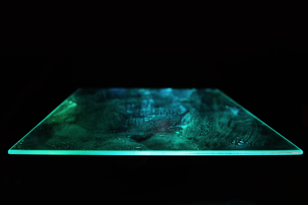
Our efforts at developing thin films on glass began several years ago when we were developing a process to cut the cost of photovoltaics. At the time, we were working with textured buffer layers of Al2O3 (sapphire) and MgO, and our efforts led to the first ever (111) c-axis oriented thin-film insulator on soda-lime glass. This was a key milestone, as this orientation can greatly improve the electronic performance of a material.
Other groups have also produced textured films. However, they used ion-beam-assisted deposition, which is much more expensive than our patented approach: electron beam evaporation.
The initial films of MgO were far better than we had hoped for. We expected to see a single peak in the X-ray diffraction scan, to indicate high texture. But we also found a second peak. This parallel peak of (111), namely (222), revealed growth of MgO (111) with almost perfect crystalline (111) alignment along the c-axis.
Figure 1. Transmission electron microscopy of 7 μm MgO film on soda-lime glass grown at 450°C showing aligned atoms which are indicative of texture.
Since then, we have scrutinised our films with the likes of transmission electron microscopy (see Figures 1 and 2), electron backscattered diffraction (see Figure 3), optical transparency (see Figure 4), and adhesion tests. Together, these techniques revealed that the MgO has high texture, complete transparency and good adhesion to the soda-lime glass. Its only inferiority to MgO formed by ion-beam-assisted deposition is that the more expensive process produces films with a bi-axial orientation. This gives the subsequent layers a biaxial texture, and an even better crystalline quality than the ones that we grow by electron-beam evaporation.
When developing photovoltaics, we have found that electronbeam evaporation can form a buffer layer with texture that is preferably (111) oriented. This is highly desirable, because it could lead to the growth of textured silicon or germanium films that boost efficiency. We have also observed that if aluminium is added during the low-temperature crystalline growth, the film that's formed is p-type, and can serve as the bottom conducting layer in a p-n junction.
Figure 2. Transmission electron microscopy cross-section of the MgO (111) film on soda-lime glass at 450 °C.
Within such a structure, an insulating MgO layer can act as a diffusion layer and texture promoter for the aluminium-silicon thin-film. It is also possible to grow silicon single crystal nanowires on the MgO. Note that aligning these nanowires perpendicular to the substrate is aided by the (111) orientation of the film since nanowires are grown in the (111) direction.
The MgO that we grow has parallels with c-axis aligned, crystalline indium gallium zinc oxide, the growth of which has been pioneered by Shunpei Yamazaki's group at the Semiconductor Energy Laboratory, Japan. Like our MgO, indium gallium zinc oxide is textured out-of-plane, but not inplane "“ that is, the crystals are aligned along the c-axis but not the a-b axis. However, indium gallium zinc oxide differs from our MgO, because it is not polycrystalline along the a-b axis. There is also another crucial difference: indium gallium zinc oxide is a semiconductor, while MgO is an insulator. So, in the display industry, MgO could serve as an insulating layer in the thin-film transistors used in displays, while indium gallium zinc oxide can form the channel of this device.
We are very excited by this opportunity. The display industry currently uses two kinds of insulator materials: SiO2 and SiNx. Neither are crystalline, let alone textured. Switching to our material would be revolutionary. It would open the door to textured silicon films that promise far higher electron mobilities, thanks to the lower angles of the grain boundaries.
Note that this is the first ever report of an insulating film grown with a (111) orientation. Back in 2005, a team at the National Renewable Energy Laboratory adopted a similar approach, but produced CeO2 (100), textured bi-axially.
Another breakthrough of ours is the annealing of the silicon film by an excimer laser. This is not trivial "“ it creates the possibility of being able to grow a highly oriented silicon thin-film channel by excimer laser annealing in a new, modified, low-temperature polysilicon process.
In the scheme, the layer of MgO (111) not only induces (111) ordered grains in the silicon film, but also protects the glass substrate from the heat generated by the annealing process. The upshot is that it allows the use of cheap soda-lime glass.
This promise has caught the eye of a major display company. They are testing our technology, and are highly encouraged by preliminary results of laser annealing of a 50 nm-thick film of a-Si:H on textured MgO (111)/soda-lime glass.
Growing III-Vs
Earlier this year, we received a patent for the growth of III-Vs on thin films of silicon on textured MgO. This process exploits the formation of a eutectic alloy consisting of III-Vs, such as gallium, combined with either silicon or germanium, deposited by either electron-beam evaporation or sputtering.
When gallium forms on the silicon layer, after diffusing to the surface of the gallium-silicon eutectic alloy, nitrogen can be introduced to the gallium to form GaN by carefully selecting the precursors. GaN forms on the highly crystalline film (or if indium and a phosphor precursor are chosen, then it is InP). It is probably not possible to form GaN at a low temperature. However, thanks to the very high melting point of MgO "“ it is over 2800 °C "“ the deposition temperature can be increased significantly when a suitable glass substrate is chosen (perhaps Lotus NXT).

Figure 3: Electron Backscatter Diffraction (EBSD) of 7 μm MgO film on soda-lime glass at 450°C. The image clearly shows that the grains (crystals) of the film are highly oriented along the (111) plane.
This approach does not lend itself to subsequent laser lift off. However, that's not necessarily an impediment, because the very thin layers of both silicon and GaN could have advantages, depending on the device needed.
If our technology is used to make LEDs, this would allow these devices to be fully integrated "“ there is no need to transfer them elsewhere. All the materials would be grown directly on the glass substrate. As the underlying silicon thin-film is textured, the silicon channel mobility could potentially approach that of a single-crystal CMOS thin-film transistor, and the final screen size could be less than 1 inch (due to the tighter integration). This approach could potentially also be applied to 5G wireless technology where GaN-on-silicon is already being explored with great interest.
Figure 4: MgO has high transparency across a wide spectral range. Transmission measurements were also taken and are estimated to be 89 percent.
Encouraging, we have just reported a mobility of 188 cm2 V-1 s-1 in silicon films made from a eutectic alloy. This result is with a polycrystalline MgO film, and we are convinced that an even higher value is possible with a textured buffer layer.
Another encouraging result is the growth of Al2O3 (111) on MgO (111)/glass, using a temperature above 600 °C. In principle, GaN could be grown on the Al2O3 (111), thereby providing another alternative to the sapphire wafer.
There is no doubt that there is much to like about replacing wafers of silicon and sapphire with crystalline thin-films made from silicon or germanium. This could trim the costs associated with the production of LEDs, and in particular, microLEDs. However, while much progress has been made, there is still more work to do.


