Loading...
News Article

SemiGen Announces New Foundry Capabilities

News

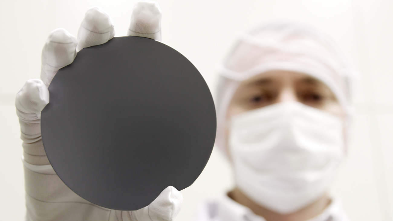
US-based SemiGen has announced that after moving into a new state-of-the art facility it has increased its foundry and screening capabilities. It now offers wafer processing of 100 to 150 mm silicon wafers, as well as alumina and aluminum nitride substrates up to just over 100mm (4.25 inches).

Services provided include any combination of photolithography, wet etch, dry etch, metallisation, grinding, polishing, as well as in-process metrology.

Recent investments in RF Test and Hi-Reliability environmental test capabilities has also enabled SemiGen to offer solutions for High-Reliability screening of amplifiers, FETs, MMICs, transistors, diodes, and other active and passive circuits and components.

Tests are performed and are delivered with full documentation in accordance with MIL-PRF-19500, MIL-PRF-38534, and MIL-PRF-38535 requirements. Element evaluation and screening options from Class H, Class K, TX, TXV, S-level, as well as custom SCD driven requirements are available.

SemiGen will be at the International Microwave Symposium June 12th to the 14th 2018.

Double heterostructure HEMTs for handsets
AlixLabs to collaborate with Linköping University
SiC MOSFETs: Understanding the benefits of plasma nitridation
Wolfspeed reports Q2 results
VueReal secures $40.5m to scale MicroSolid printing
Mitsubishi joins Horizon Europe's FLAGCHIP project
Vishay launches new high voltage SiC diodes
UK team leads diamond-FET breakthrough
GaN adoption at tipping point, says Infineon
BluGlass files tuneable GaN laser patents
QD company Quantum Science expands into new facility
Innoscience files lawsuit against Infineon
Riber revenues up 5% to €41.2m
Forvia Hella to use CoolSiC for next generation charging
Photon Design to exhibit QD simulation tool
Ortel transfers CW laser fabrication to Canada
Luminus adds red and blue multi-mode Lasers
PseudolithIC raises $6M for heterogeneous chiplet tech
Mesa sidewall design improves HV DUV LEDs
IQE revenue to exceed expectations
'Game-changing' VCSEL system targets clinical imaging
German start-up secures finance for SiC processing tech
Macom signs preliminaries for CHIPS Act funding
IQE and Quintessent partner on QD lasers for AI
EU funds perovskite tandems for fuel-free space propulsion
EU to invest €3m in GeSi quantum project
Transforming the current density of AlN Schottky barrier diodes
Turbocharging the GaN MOSFET with a HfO₂ gate
Wolfspeed launches Gen 4 SiC MOSFET technology
Report predicts high growth for UK's North East
Element Six unveils Cu-diamond composite
SemiQ launches hi-rel 1700V SiC MOSFETs
×
Search the news archive

To close this popup you can press escape or click the close icon.
Logo
x
Logo
×
Register - Step 1

You may choose to subscribe to the Compound Semiconductor Magazine, the Compound Semiconductor Newsletter, or both. You may also request additional information if required, before submitting your application.


Please subscribe me to:


You chose the industry type of "Other"

Please enter the industry that you work in:
 
x