
Culprit of some GaN defects could be nitrogen
As silicon-based semiconductors reach their performance limits, GaN is becoming the next go-to material to advance LED technologies, high-frequency transistors and photovoltaic devices. Holding GaN back, however, is its high numbers of defects.
The material degradation is due to dislocations - when atoms become displaced in the crystal lattice structure. When multiple dislocations simultaneously move from shear force, bonds along the lattice planes stretch and eventually break. As the atoms rearrange themselves to reform their bonds, some planes stay intact while others become permanently deformed, with only half planes in place. If the shear force is great enough, the dislocation will end up along the edge of the material.
Layering GaN on substrates of different materials makes the problem that much worse because the lattice structures typically don't align. This is why expanding our understanding of how GaN defects form at the atomic level could improve the performance of the devices made using this material.
A team of researchers has taken a significant step toward this goal by examining and determining six core configurations of the GaN lattice. They presented their findings in the Journal of Applied Physics.
"The goal is to identify, process and characterize these dislocations to fully understand the impact of defects in GaN so we can find specific ways to optimize this material," said Joseph Kioseoglou, a researcher at the Aristotle University of Thessaloniki and an author of the paper.
There are also problems that are intrinsic to the properties of GaN that result in unwanted effects like colour shifts in the emission of GaN-based LEDs. According to Kioseoglou, this could potentially could be addressed by exploiting different growth orientations.
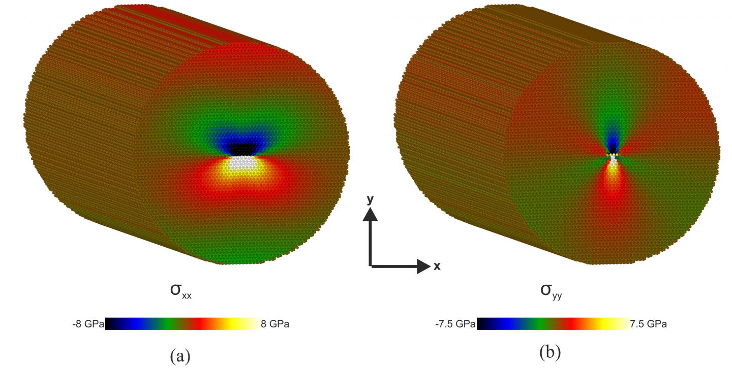
The researchers used computational analysis via molecular dynamics and density functional theory simulations to determine the structural and electronic properties of a-type basal edge dislocations along the <1-100> direction in GaN. Dislocations along this direction are common in semipolar growth orientations. The image above shows the distribution of stresses per atom (a) and (b) of a-edge dislocations along the <1-100> direction in wurtzite GaN.
The researchers found that the N polarity configurations exhibited significantly more states in the bandgap compared to the Ga polarity ones, with the N polar configurations presenting smaller bandgap values.
"There is a connection between the smaller bandgap values and the great number of states inside them," said Kioseoglou. "These findings potentially demonstrate the role of nitrogen as a major contributor to dislocation-related effects in GaN-based devices."
'Structural and electronic properties of a-edge dislocations along <1-100> in GaN' by Stefanos Giaremis et al; Journal of Applied Physics June 26, 2018,


