
Polarisation Breakthrough could Enhance PV Tech
III-Nitride compound materials have attracted a great deal of attention for harvesting solar energy due to their outstanding physical and chemical stabilities, radiation resistance, high light absorption capability and ability to cover spectral range from UV to near infrared region (∼0.64eV to ∼3.4eV). However, conversion efficiencies in planar GaN/InGaN solar cells suffer due to the detrimental effect of polarisation charges.
Now a team of researchers from National Institute of Technology Silchar, India and SRM University, India has proposed an alternative to the planar type approach that uses a new structure based on III-Nitride nanowires to reduce the polarisation effect and achieve higher efficiencies.
They believe a GaN/InGaN nanowire solar cell with multiple quantum wells (i.e. a thick intrinsic InGaN layer) could solve the problem due to its partially relaxed stress and strain effect, efficient carrier collection into orthogonal spatial direction, efficient light trapping, and low dislocation density due to the free standing substrate.
Radial GaN/InxGa1−xN nanowires have already been proven in high frequency, high power transistor, photo detector, LED and laser applications but exploitation of nanowires for photovoltaic applications is still in its infancy.
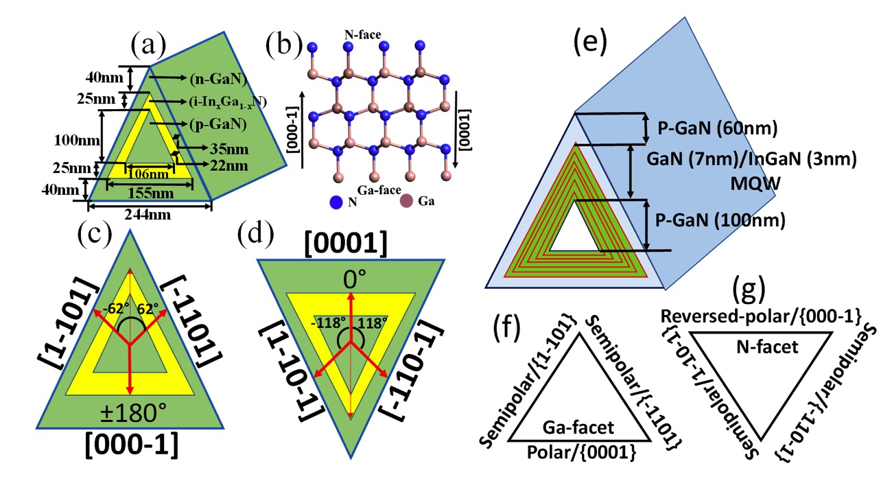
Previously, the same team has studied different types of GaN/InGaN/GaN core/shell/shell type nanowires and concluded that III-Nitride nanowires possess either a hexagonal or a triangular cross-section and that these influence polarisation charges in complex ways.
A further exploration of the piezo-phototronics effect (a three way coupling effect of piezoelectric, semiconductor and photonic properties in non-central symmetric semiconductor materials) in the triangular nanowire-type solar cells found that polarisation charges are more optimised in triangular geometries than hexagonal ones. The geometrical advantage of triangular nanowires is absent in hexagonal nanowires.
Depending on the growth conditions, the geometry of triangular nanowires may have two distinct set of crystal planes of either {0001}, {1-10-1}, {-110-1} or {000-1}, {1-101}, {-1101} as shown in Fig. 1(b) and (c).
The researchers discovered that triangular nanowires with the second configuration of facets {000-1}, {1-101}, {-1101} are more efficient in capturing photons from sunlight and converting it to current than the first configuration. It is due to the presence of reversed polar plane {000-1} which has opposite polarity of charges to the {0001} facet but similar in magnitude.
Additionally, team also proposed to incorporate multiple quantum wells (MQW) along all the facets of nanowires. They observed the effects of polarisation charges on carrier escape and collection.
The analysis reveals that the crystallographic orientation and polarisation field have a complex dependency in MQW based III-Nitride nanowires solar cell and can only be clearly interpreted via numerical simulation. It suggests that implementation of QWs in {000-1} facets of nanowires is quite efficient for carrier separation, whereas, the {0001} plane is detrimental for solar cell performance due to opposite polarisation of ions.
By efficient utilisation of polarisation charges, the researchers achieved a power conversion efficiency of 9.82 percent with high fill factor (94.34 percent) and more than 70 percent quantum efficiency from the 7 MQWs based nanowire solar cell with 10 percent indium content, 90 percent gallium.
This novel concept and findings provide new scope for future high-efficiency III-Nitride nanowires solar cell for space as well as terrestrial applications.
'Polarization Charges in High Performance GaN/InGaN Core/Shell Multiple Quantum Well Nanowire for Solar Energy Harvesting', by S. R. Routray and T. R. Lenka; IEEE Transaction on Nanotechnology, 18 June 2018


