Fujitsu Triples Output Power of GaN Transistors

Fujitsu has developed a crystal structure that both increases current and voltage in GaN HEMTs effectively tripling the output power of transistors used for transmitters in the microwave band.
The GaN HEMT technology can serve as a power amplifier for equipment such as weather radar - by applying the developed technology to this area, it is expected that the observation range of the radar will be expanded by 2.3 times, enabling early detection of cumulonimbus clouds that can develop into torrential rainstorms.
To expand the observation range of equipment like radar, it is essential to increase the output power of the transistors used in power amplifiers. With conventional technology, however, applying high voltage could easily damage the crystals that compose a transistor. Therefore, it was technically difficult to increase current and voltage simultaneously, which is required to realize high-output power GaN HEMTs.
Fujitsu and Fujitsu Laboratories have developed a crystal structure that improves operating voltage by dispersing the applied voltage to the transistor, and thereby prevents crystal damage (patent pending). This technology has enabled Fujitsu to successfully achieve the world's highest power density at 19.9 watts per millimeter of gate width for GaN HEMT employing InAlGaN barrier layer.
This research was partially supported by Innovative Science and Technology Initiative for Security, established by the Acquisition, Technology & Logistics Agency (ATLA) of the Japanese Ministry of Defense.
Details of this technology will be announced at the International Symposium on Growth of III-Nitrides (ISGN-7), an international conference about nitride semiconductor crystal growth, held in Warsaw, Poland, from August 5-10.
Development Background
In recent years, GaN HEMTs have been widely used as high-frequency power amplifiers in long-distance radio wave applications, such as radars and wireless communications. It is also expected that they will be used for weather radars to accurately observe localized torrential rainfall, as well as in millimeter-waveband wireless communications for fifth-generation mobile communications (5G). The outreach of microwaves from the microwave and millimeter-wave bands used for radar and wireless communications can be extended by increasing the output power of the high-frequency GaN HEMT power amplifiers used for transmitter. This allows for expanded radar observation range as well as longer distance and higher capacity communications.
Fujitsu Laboratories has been conducting research on GaN HEMTs since the early 2000's, and currently provides the AlGaN HEMTs used in a variety of areas. Recently, Fujitsu Laboratories has been conducting research on InAlGaN HEMTs as a new generation GaN HEMT technology, which enables high current operation as high-density electrons become available. Accordingly, Fujitsu and Fujitsu Laboratories have developed a crystal structure that achieves both high current and high voltage simultaneously.
Issues
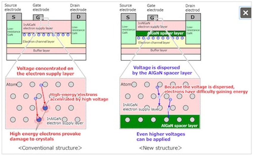
In order to improve the output power of a transistor, it is required to realize both high current and high voltage operation. Research is ongoing for InAlGaN HEMTs for the next generation GaN HEMT that would contribute to increased current, as InAlGaN HEMTs can increase electron density within the transistor. When high voltage is applied, however, an excessive amount of voltage becomes concentrated on a part of the electron supply layer, damaging the crystals within transistors. Consequently, these transistors had a serious issue whereby their operating voltage could not be increased (Figure 1 above, shows the mechanism of crystal damage and the newly developed crystal structure).
About the Newly Developed Technology
Fujitsu and Fujitsu Laboratories have succeeded in developing a transistor that can provide both high current and high voltage by inserting a high-resistance AlGaN spacer layer between the electron supply layer and the electron channel layer.
For conventional InAlGaN HEMTs, all of the applied voltage between the gate and drain electrodes were applied to the electron supply layer, and numerous electrons having high kinetic energy were generated in the electron supply layer. Subsequently, these electrons would violently strike the atoms which compose the crystal structure, causing damage. As a result of this phenomenon, there was a limit to the maximum operating voltage of the transistor.
By inserting the newly developed high-resistant AlGaN spacer layer, the voltage within the transistor can be dispersed across both the electron supply layer and the AlGaN spacer layer. By mitigating the concentration of voltage, the kinetic energy increase of the electrons within the crystal is suppressed and damage to the electron supply layer can be prevented, leading to an improved operating voltage of up to 100 volts. This operation voltage corresponds to over 300,000 volts if the distance between the source electrode and gate electrode is one centimetre.
Effects
By inserting this newly developed AlGaN spacer layer in InAlGaN HEMTs, Fujitsu and Fujitsu Laboratories have achieved both high current and high voltage operation, which was conventionally difficult to achieve. Furthermore, by applying the single-crystal diamond substrate bonding technology Fujitsu developed in 2017, the heat generation within the transistor can be efficiently dissipated through diamond substrate, enabling stable operations.
When GaN HEMTs with this crystal structure were measured in actual tests, they successfully achieved the world's highest output power of 19.9 watts per millimeter of gate width, which is three times higher than the output power of conventional AlGaN/GaN HEMTs. the figure above shows the newly developed GaN HEMT transistor structure and a comparison of output power against conventional technology.
Future plans
Fujitsu and Fujitsu Laboratories will conduct an evaluation of the heat resistance and output performance of GaN HEMT power amplifiers using this technology, with the goal of commercializing high output power, high frequency GaN HEMT power amplifiers for use in applications such as radar systems, including weather radar, and 5G wireless communication systems by fiscal 2020.


