
Watching 2D materials grow
2D materials are crystals which consist of only one or a few layers of atoms. They are among the thinnest structures on earth and often display unusual properties, promising new applications in opto-electronics and energy technology. But their production is difficult and the crystallisation process depends on many different factors.
In the past, different techniques have yielded quite diverse results, but the reasons for this could not be accurately explained. Thanks to a new method developed by research teams at TU Wien, the University of Vienna and Joanneum Research in Styria, for the first time ever it is now possible to observe the crystallisation process directly under the electron microscope using the 2D semiconductor MoS2, an atomically thin layer of molybdenum and sulphur atoms. The method has now been presented in the scientific journal ACS Nano.
From gas to crystal
"MoS2 can be used in transparent and flexible solar cells or for sustainably generating hydrogen for energy storage", says the lead author of the study, Bernhard C. Bayer from the Institute of Materials Chemistry at TU Wien. "In order to do this, however, high-quality crystals must be grown under controlled conditions."
Usually this is done by starting out with atoms in gaseous form and then condensing them on a surface in a random and unstructured way. In a second step, the atoms are arranged in regular crystal form - through heating, for example. "The diverse chemical reactions during the crystallisation process are, however, still unclear, which makes it very difficult to develop better production methods for 2D materials of this kind", Bayer says.
Thanks to a new method, however, it should now be possible to accurately study the details of the crystallisation process. "This means it is no longer necessary to experiment through trial and error, but thanks to a deeper understanding of the processes, we can say for certain how to obtain the desired product", Bayer adds.
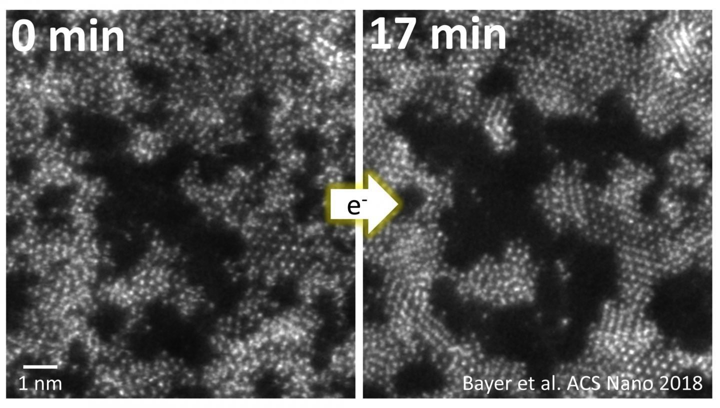
Graphene as a substrate
First, molybdenum and sulphur are placed randomly on a membrane made of graphene. Graphene is probably the best known of the 2D materials - a crystal with a thickness of only one atom layer consisting of carbon atoms arranged in a honeycomb lattice. The randomly arranged molybdenum and sulphur atoms are then manipulated in the electron microscope with a fine electron beam. The same electron beam can be used simultaneously to image the process and to initiate the crystallisation process.
That way it has now become possible for the first time to directly observe how the atoms move and rearrange during the growth of the material with a thickness of only two atomic layers. The picture above shows how at first the atoms are randomly distributed, then after being manipulated with the electron beam they form crystal structures (right).
"In doing so, we can see that the most thermodynamically stable configuration doesn't necessarily always have to be the final state", Bayer says. Different crystal arrangements compete with one another, transform into each other and replace one another. "Therefore, it is now clear why earlier investigations had such varying results. We are dealing with a complex, dynamic process," says Bayer.
The new findings will help to adapt the structure of the 2D materials more precisely to application requirements in future by interfering with the rearrangement processes in a targeted manner.
'Atomic-Scale in Situ Observations of Crystallisation and Restructuring Processes in Two-Dimensional MoS2 Films' by Bayer et al; ACS Nano, (2018), 12, 8758-8769


