
Siltectra Ramps Up Wafering Services
Siltectra, a German wafering technology company, will begin offering "˜outsourced wafering' services to customers, starting in January 2019. The new business aims to provide affordable access to the company's breakthrough Cold Split wafering solution to global semiconductor manufacturers and materials providers, and help speed the adoption of new substrate materials by the industry at large. The manufacturing initiative will be located at Siltectra's headquarters in Dresden.
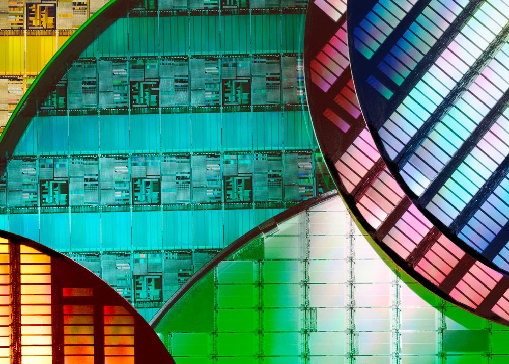
The first phase of the new business will concentrate on 6-inch SiC wafers. This focus responds to early requests for the new wafering service from manufacturers of SiC-substrates for applications like electric vehicles and 5G technology. The SiC market is expected to grow steadily between now and 2022, with demand from customers in the US, Europe and China, and strong momentum in Japan. Siltectra will begin by producing 500 wafers per week, with plans to increase the volume to 2000 wafers per week by the end of 2019.
Cold Split is a high-output, low-cost wafering and thinning technology for substrates like SiC and GaAs, as well as GaN, sapphire and silicon. The laser-based technique employs a chemical-physical process that uses thermal stress to generate a force that splits the material with exquisite precision along the desired plane, and produces virtually no kerf loss. The "˜no kerf loss' capability is unique to Cold Split and delivers breakthrough advantages. First, it extracts more wafers per boule than conventional wafering technologies. This drives up output. Second, it dramatically reduces consumables costs.
In addition to semiconductor customers, Siltectra will also make the service available to materials manufacturers who stand to gain from Cold Split's technical and economic advantages. The economic benefits are derived from higher output (up to 2X from the same amount of material), as well as lower capex burdens (furnaces, for instance). The technology benefits are derived from Cold Split's inherent capabilities, which includes better depth-of-focus stability for the lithography process which is enabled by edge flatness parameters that are superior to the standard lapping process. In addition, the geometrical profile for Cold Split wafers is better suited for lateral processes, especially epitaxy.
The new "˜outsourced wafering' business is a central component of Siltectra's growth strategy. The company began preparing earlier this year when it expanded its Dresden facility and created a dedicated manufacturing space. In addition, Siltectra invested in new process equipment, pioneered new automation techniques, hired additional technologists, and launched a pilot production line. During this time, Siltectra also continued to boost Cold Split's capabilities by adding enabling hardware, software and process innovations. The new innovations further enriched the company's global IP portfolio which today consists of 70 patent families containing 200 patents in total.
"Outsourced wafering services is a natural next step for Siltectra and we're excited by the enthusiasm we're hearing from semiconductor manufacturers, as well as materials providers," said the company's Head of Business Development, David Schneider. "It's a compelling service offering for substrate manufacturers seeking an affordable portal to an ultra-high-output wafering solution. Early feedback confirms that customers value the access to Cold Split's unique innovations and Siltectra's process expertise, and appreciate our knowledge and experience with diverse substrate materials. We intend to meet their wafering needs with a scalable business plan, starting with one shift and adding additional shifts as demand grows."


