Loading...
News Article

Trymax wins order from Chinese CS foundry

News
NEO 2000 Series plasma tool chosen to perform photoresist ashing and descum on substrates

Trymax Semiconductor Equipment BV, a plasma company based in the Nerthelands, has received multi-system orders for its NEO 2000 Series from a Chinese compound semiconductor foundry. Shipping of the first systems will be in Q4 2018 and continue during Q1 2019.

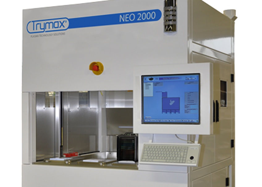
Trymax's NEO 2000 Series was selected by the customer to perform photoresist ashing and descum on SiC and LiTaO3 substrates. Main end applications will be in the field of RF and power electronics that are both facing significant growth driven by the IoT, 5G, and automotive.

The NEO 2000 Series is described as a high throughput and low cost of ownership dual chamber system. It will be configured with both high and low temperature plasma chambers and process wafers from 4 up to 8inches. These multi-system orders come in addition of previous multi-system orders received by Trymax from the same customer a few years ago.

"We are thankful by this strong vote of confidence in our state-of-the-art solutions" stated Ludo Vandenberk, executive VP of Trymax. "Partnership and best-in-class customer support has been key values of Trymax since the beginning of the company's operations. Winning this additional business confirms our strategy is right and we look forward to supporting our customer growing its business".

Trymax will be exhibiting at SEMICON Europa in Munich (Germany) from November 13 to 16th 2018.

Double heterostructure HEMTs for handsets
AlixLabs to collaborate with Linköping University
SiC MOSFETs: Understanding the benefits of plasma nitridation
Wolfspeed reports Q2 results
VueReal secures $40.5m to scale MicroSolid printing
Mitsubishi joins Horizon Europe's FLAGCHIP project
Vishay launches new high voltage SiC diodes
UK team leads diamond-FET breakthrough
GaN adoption at tipping point, says Infineon
BluGlass files tuneable GaN laser patents
QD company Quantum Science expands into new facility
Innoscience files lawsuit against Infineon
Riber revenues up 5% to €41.2m
Forvia Hella to use CoolSiC for next generation charging
Photon Design to exhibit QD simulation tool
Ortel transfers CW laser fabrication to Canada
Luminus adds red and blue multi-mode Lasers
PseudolithIC raises $6M for heterogeneous chiplet tech
Mesa sidewall design improves HV DUV LEDs
IQE revenue to exceed expectations
'Game-changing' VCSEL system targets clinical imaging
German start-up secures finance for SiC processing tech
Macom signs preliminaries for CHIPS Act funding
IQE and Quintessent partner on QD lasers for AI
EU funds perovskite tandems for fuel-free space propulsion
EU to invest €3m in GeSi quantum project
Transforming the current density of AlN Schottky barrier diodes
Turbocharging the GaN MOSFET with a HfO₂ gate
Wolfspeed launches Gen 4 SiC MOSFET technology
Report predicts high growth for UK's North East
Element Six unveils Cu-diamond composite
SemiQ launches hi-rel 1700V SiC MOSFETs
×
Search the news archive

To close this popup you can press escape or click the close icon.
Logo
x
Logo
×
Register - Step 1

You may choose to subscribe to the Compound Semiconductor Magazine, the Compound Semiconductor Newsletter, or both. You may also request additional information if required, before submitting your application.


Please subscribe me to:


You chose the industry type of "Other"

Please enter the industry that you work in: