
This article was originally featured in the edition:
PIC Magazine Issue 8 - March 2018
Micro-LEDs with mammoth potential
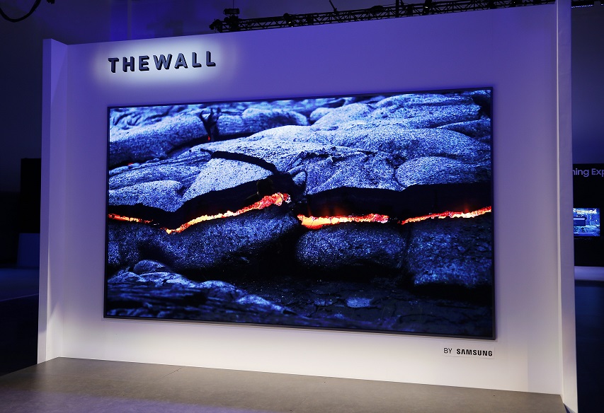
In September, South Korean electronics giant, LG, introduced a gargantuan 175-inch microLED TV for ultra-large display applications, in response to Samsung's 146-inch beast, 'The Wall', launched in January this year.
As display markets get ready for, literally, the next big technology, Samsung has secured its supply of micro-LEDs from Taiwan-based PlayNitride while industry reports indicate LG is sourcing chips from Epistar, Taiwan, and HC SemiTek, China.
"This industry sector is in its early stages but is growing and developing very, very fast," highlights n-tech Research analyst, Boris Kobrin. "Commercialisation has only started this year but all the major display businesses and OEMS are working on prototypes, which are now being brought to the market."
Micro-LEDs based on InGaN semiconductors and developed by Hongxing Jiang and Jingyu Lin, then at US-based Kansas State University, first emerged at the turn of this century. Research swiftly continued far and wide and come 2012, Sony had released its 55-inch 'Crystal LED Display', comprising around 6 million microLEDs. Larger iterations have followed from Sony, Samsung and now LG, while industry players keenly anticipate further devices from Apple and Facebook.
"Scalability is the draw for micro-LEDs in these extra-large displays," points out Kobrin. According to the analyst, next generation digital cinemas demand high dynamic range, super-high density, high brightness and contrast displays that state-of-the-art projectors and screens just can't offer. Meanwhile, laser colour video displays are expensive, while manufacturing OLED displays beyond some 65 inches is technically challenging as well as costly.
"However, microLEDs offer extraordinary contrast, brightness and scalability," says Kobrin. "More than 98% of a pixel is empty space, as the tiny pixel contains a very tiny microLED... so [system] cost doesn't scale with area, it actually scales with resolution, which is a big deal for these huge-area displays."
"Displays in digital cinemas and home theatres are going to be dominated by micro-LEDs due to these capabilities that you just cannot find in any other technology, not even the OLED," he adds.
But micro-LEDs markets are not all about size. While the latest TV behemoths promise higher-than OLED brightness at a near-LCD cost, the actual micro-LED also provides tip top power efficiency, high contrast, high brightness and a longer lifetime than the OLED.
Given this, Kobrin reckons the near-eye augmented reality/virtual reality projector market is one to watch. "This application requires very high resolution, high brightness and contrast as well as low weight and a small form factor," he says. "The micro-LED provides all of these needs very well."
Factor in anticipated demand from the smart watch market as well as automotive head-up displays, and Kobrin predicts that the global micro-LED market will swell from $2.7 billion in revenue in 2019, to a hefty $10.7 billion in 2022. Still, challenges exist.
Quality variability across GaN wafers has plagued manufacturers, although, for example, companies such as US-based Optovate are developing selective array transfer processes to deal with this issue. At the same time, problems over display drivers as well as faltering efficiencies for smaller micro-LEDs are also reportedly being solved.
For Kobrin, a key issue has been 'mass transfer'. Super-high resolution, contrast and brightness applications, namely extra-large displays and near-eye AR/VR projectors, require very high pixel density displays that are difficult to manufacture using traditional pick and place transfer processes.
Here, the microLED display is assembled, one sub-pixel at a time, onto a CMOS backplane, which for, say a 4K television with some 25 million sub-pixels is time-consuming and expensive. What's more, many pick and place processes can, at best, only handle 50 micron pixels, but future displays will house pixels with smaller diameters.
Thankfully, as Kobrin highlights, myriad companies have been springing up to deliver a range of mass transfer manufacturing processes in which thousands and thousands of sub-pixels are simultaneously moved from a sapphire or silicon donor carrier to the display substrate.
For example, US start-up, Uniqarta, has developed a 'Laser Enabled Advanced Placement' process in which a laser transfers dies from a carrier to a substrate at a rate of up to 100 million units an hour, orders of magnitude higher than traditional pick and place processes.
Meanwhile SelfArray, US, is pioneering a 'directed self-assembly' process in which LED dies, covered with a pyrolitic graphite film and placed onto a vibrating magnetic stage, align with the magnetic field, and are then transferred to the display substrate.
The company claims, once mature, the technology will manufacture a 4K TV in minutes.
"We need to see huge numbers of chips being transferred, even for small devices," says Kobrin. "The finished technology does not exist, but companies are developing processes and I would expect to see some of these acquired by large corporations, such as Facebook and Google."
"It is also not yet obvious which technology will win but to me, it looks like the laser-based transfer technologies have the advantage," he adds.
But as issues are ironed out one by one, supply chain chinks remain under close review by many in the industry. It's no secret that the complex and lengthy micro-LED display supply chain remains fragmented as combining LED production with display manufacturing and assembly has not been easy.
"It is not certain at this point how this issue will play out," says Kobrin. "Will the large players take charge and create a vertically integrated structure... or will the semiconductor foundries reconfigure and update lines with the required epitaxial growth? This now needs to be seen."


